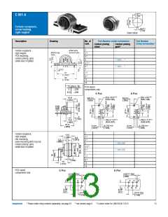
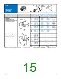
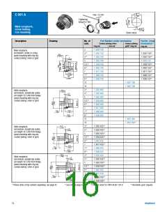
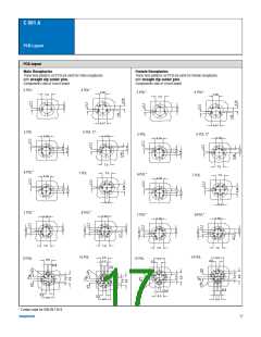
C 091 A
PCB-Layout
PCB-layout
Male Receptacles
Female Receptacles
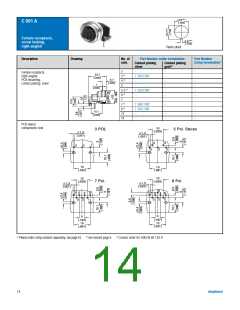
These hole patterns on PCB are valid for male receptacles
with straight dip solder pins.
These hole patterns on PCB are valid for female receptacles
with straight dip solder pins.
Components side of circuit board
Components side of circuit board
3 POL*
4 POL*
4,26
2
3 POL*
4 POL*
7,0
4,26
3
7,0
3
3
4
3
2
1
2
1
1
1
2
4
6,47
6,47
5 POL
6 POL*
7 POL*
5 POL S*
5 POL
6 POL*
7 POL*
5 POL S*
6,06
3
4,95
2
4,95
2
6,06
3
5
3
4
1
4
4
1
5
3
2
2
4
5
1
1
5
7,0
7,0
7,0
7,0
7 POL
7 POL
6,06
6,06
3
7
4
4
7
3
3
6
2
5
3
6
5
2
4
2
6
1
2
4
1
6
5
1
1
5
3,5
3,5
8 POL*
8 POL*
4,95
4,95
4,95
2
4,95
2
2
5
5
2
4
4
4
1
4
5
5
3
3
3
1
1
1
8
3
7
6
8
7
6
6
7
6
7
7,0
7,0
7,0
9,0
7,0
14 Pol.
14 POL
12 Pol.
14 POL
14 Pol.
9,0
12 POL
12 POL
6,0
3,0
4,5
3,0
0,8
G
G
B
C
H
F
H
J
M
N
J
M
K
E
D
K
F
E
O
L
L
A
D
A
D
L
L
D
A
K
F
N
M
E
K
H
B
C
B
C
J
F
H
G
0,8
0,8
3,0
4,5
6,0
6,0
3,0
9,0
9,0
* Contact order for DIN EN 130-9
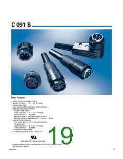
Amphenol
17

 AMPHENOL [ Amphenol ]