AMD
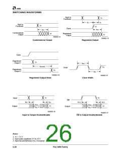
SWITCHING WAVEFORMS
Input or
Feedback
VT
tH
tS
Input or
Feedback
VT
VT
tCO
Clock
tPD
Combinatorial
Output
Registered
Output
VT
VT
16492D-13
16492D-12
Combinatorial Output
Registered Output
Clock
Registered
Output 1
VT
tWH
tSKEWR
VT
Clock
Registered
Output 2
VT
tWL
16492D-14
16492D-15
Registered Output Skew
Clock Width
VT
VT
Input
OE
tER
tEA
tPXZ
tPZX
VT
VOH – 0.5V
VT
VOH – 0.5V
VOL + 0.5V
Output
Output
VOL + 0.5V
16492D-16
16492D-17
Input to Output Disable/Enable
OE to Output Disable/Enable
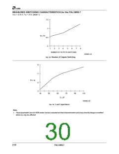
Notes:
1. VT = 1.5 V
2. Input pulse amplitude 0 V to 3.0 V
3. Input rise and fall times 2 ns–3 ns typical.
2-28
PAL16R8 Family

 AMD [ AMD ]