P R E L I M I N A R Y
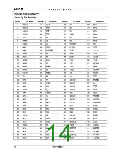
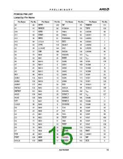
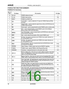
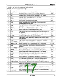
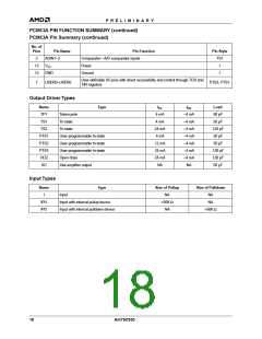
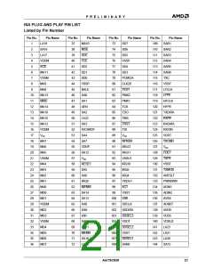
PCMCIA PIN FUNCTION SUMMARY (continued)
PCMCIA Pin Summary (continued)
No. of
Pins
Pin Name
Pin Function
Pin Style
1
1
1
1
1
TDO
TMS
Test Data Out—this is the data output signal for IEEE 1149.1 testing
Test Mode Select—this is the test mode select for IEEE 1149.1 testing
Test Reset—this is the reset signal for IEEE 1149.1 testing
User-programmable pin
TS1
I
TRST
USER7
RXC
I
PTS3
PTS3
Receive Clock—provides decode receive clock
Test pin—when asserted, this pin places the Am79C930 device into a
nonstandard factory-only test mode
1
1
TEST
I
I
Clock input to drive BIU, 80188 core, and TAI, supplying network data rate
information
CLKIN
2
1
PMX1–2
TXC
Power Management Xtal—32-kHz Xtal input for sleep timer reference
Transmit Clock—may be configured either as input or output
I/XO
TS1
Low Frequency Power Enable—used to power up the low-frequency section of
the transceiver
1
LFPE
PTS1
1
1
LFCLK
Low Frequency Clock—a reference signal for the transceiver synthesizer
Low Frequency Synthesizer Lock—a programmable signal
TS1
LLOCKE
PTS1
High Frequency Power Enable—used to power up the high-frequency section
of the transceiver
1
HFPE
PTS1
1
2
2
HFCLK
High Frequency Clock—a reference signal for the transceiver synthesizer
Antenna Select—used to select between two antennas
TS1
PTS1
ANTSLT, ANTSLT
TXCMD, TXCMD
Transmit Command—used to select the transmit path in the transceiver
TP1, PTS1
Transmit Power Enable—used to power up the transmit section of the
transceiver
1
TXPE
TP1
2
1
1
1
1
1
1
1
3
1
1
TXDATA, TXDATA
TXMOD
RXPE
Transmit Data—supplies the transmit data stream to the transceiver
Transmit Modulation Enable—enables the modulation of transmit data
Receive Power Enable—enables the receive function of the transceiver
Receive Data—accepts receive data in NRZ format from the transceiver
Frame Detect—start of frame delimiter detection indication
TP1, PTS1
TP1
PTS1
I
RXDATA
FDET
TS1
RXCIN
Receive Clock Input—optional clock input that allows for an external PLL
Serial Data Clock—clock output used to access serial peripheral devices
Serial Data Data—data pin used to access serial peripheral devices
Serial Data Select—chip select outputs used to select serial peripheral devices
Activity LED—output capable of driving an LED
IPU
SDCLK
PTS1
PTS1
PTS1
PTS2
PTS2
SDDATA
SDSEL3–SDSEL1
ACT
LNK
Link LED—output capable of driving an LED
A/D Reference—an input that can be used to set the analog reference voltage
for the internal A/D converter
1
7
ADREF
I
Serial Approximation Register—supplies the value of the serial approximation
register used in the A/D converter
SAR6–SAR0
TS1
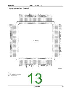
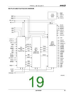
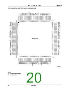
Am79C930
17

 AMD [ AMD ]