P R E L I M I N A R Y
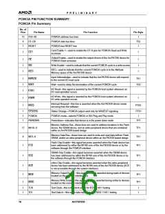
PCMCIA PIN FUNCTION SUMMARY
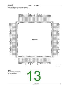
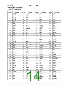
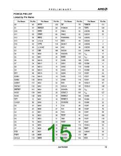
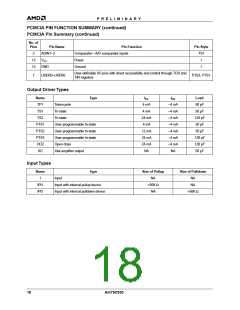
PCMCIA Pin Summary
No. of
Pins
15
8
Pin Name
A14–A0
Pin Function
Pin Style
PCMCIA address bus lines
PCMCIA data bus lines
PCMCIA bus RESET line
I
TS2
I
D7–D0
RESET
1
Card Enable 1—used to enable the D7–0 pins for PCMCIA Read and Write
accesses
1
CE1
I
Output Enable—used to enable the output drivers of the Am79C930 device for
PCMCIA Read accesses
1
1
1
OE
I
I
I
WE
REG
Write Enable—used to indicate that the current PCMCIA cycle is a write access
REG—used to indicate that the current PCMCIA cycle is to the Attribute
Memory space of the Am79C930 device
Input Acknowledge—used to indicate that the Am79C930 device will respond
to the current I/O read cycle
1
1
1
INPACK
WAIT
TS1
TS2
Wait—used to delay the termination of the current PCMCIA cycle
I/O Read—this signal is asserted by the PCMCIA host system whenever an
I/O read operation occurs
IORD
I/O Write—this signal is asserted by the PCMCIA host system whenever an
I/O write operation occurs
1
1
IOWR
IREQ
I
Interrupt Request—this line is asserted when the Am79C930 device needs
servicing from the software
PTS3
1
1
1
STSCHG
PCMCIA
PWRDWN
Status Change—PCMCIA output used only for WAKEUP signaling
PCMCIA mode—selects PCMCIA or ISA Plug and Play mode
Powerdown—indicates that device is in the power down mode
PTS1
I
TP1
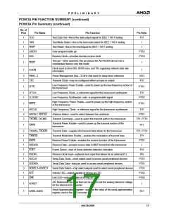
Memory Address Bus—these lines are used to address locations in the Flash
device, the SRAM device, and an extra peripheral device that are contained
within an Am79C930-based design
17
8
MA16–0
MD7–0
FCE
TP1
TS1
TP1
Memory Data Bus—these lines are used to write and read data to/from Flash,
SRAM, and/or an extra peripheral device within an Am79C930-based design
Flash Chip Enable—this signal becomes asserted when the Flash device has
been addressed by either the 80188 core of the Am79C930 device or by the
software through the PCMCIA interface
1
SRAM Chip Enable—this signal becomes asserted when the SRAM device
has been addressed by either the 80188 core of the Am79C930 device or by
the software through the PCMCIA interface
1
1
SCE
XCE
TP1
TP1
eXtra Chip Enable—this signal becomes asserted when the extra peripheral
device has been addressed by the 80188 core of the Am79C930 device (XCE
is not accessible through the system interface)
Memory Output Enable—this signal becomes asserted during reads of devices
located on the memory interface bus
1
1
MOE
MWE
TP1
TP1
Memory Write Enable—this signal becomes asserted during writes to devices
located on the memory interface bus
1
1
TCK
TDI
Test Clock—this is the clock signal for IEEE 1149.1 testing
I
I
Test Data In—this is the data input signal for IEEE 1149.1 testing
16
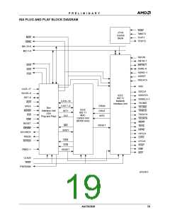
Am79C930

 AMD [ AMD ]