D A T A S H E E T
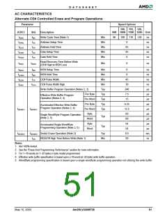
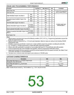
ERASE AND PROGRAMMING PERFORMANCE
Parameter
Typ (Note 1)
Max (Note 2)
Unit
sec
sec
µs
Comments
Sector Erase Time
Chip Erase Time
0.5
32
3.5
64
Excludes 00h programming
prior to erasure (Note 6)
Byte
Word
Byte
60
600
600
540
540
1200
38
Single Word/Byte Program Time (Note 3)
60
µs
54
µs
Accelerated Single Word/Byte Program Time
(Note 3)
Word
54
µs
Total Write Buffer Program Time (Note 4)
Effective Write Buffer Program Time (Note 5)
240
7.5
15
µs
Excludes system level
overhead (Note 7)
Per Byte
Per Word
µs
75
µs
Total Accelerated Write Buffer Program Time (Note 4)
200
6.25
12.5
31.5
1040
33
µs
Per Byte
Per Word
µs
Effective Accelerated Write Buffer Program Time
(Note 5)
65
µs
Chip Program Time
73
sec
Notes:
1. Typical program and erase times assume the following conditions: 25°C, 3.0 V VCC, Programming specification assume that
all bits are programmed to 00h.
2. Maximum values are measured at VCC = 3.0, worst case temperature. Maximum values are valid up to and including 100,000
program/erase cycles.
3. Word/Byte programming specification is based upon a single word/byte programming operation not utilizing the write buffer.
4. For 1-16 words or 1-32 bytes programmed in a single write buffer programming operation.
5. Effective write buffer specification is calculated on a per-word/per-byte basis for a 16-word/32-byte write buffer operation.
6. In the pre-programming step of the Embedded Erase algorithm, all bits are programmed to 00h before erasure.
7. System-level overhead is the time required to execute the command sequence (s) for the program command. See Tables 12 and
13 for further information on command definitions.
8. The device has a minimum erase and program cycle endurance of 100,000 cycles.
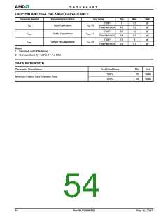
LATCHUP CHARACTERISTICS
Description
Min
Max
Input voltage with respect to VSS on all pins except I/O pins
(including A9, OE#, and RESET#)
–1.0 V
12.5 V
Input voltage with respect to VSS on all I/O pins
–1.0 V
VCC + 1.0 V
+100 mA
V
CC Current
–100 mA
Note: Includes all pins except VCC. Test conditions: VCC = 3.0 V, one pin at a time.
May 16, 2003
Am29LV320MT/B
53

 AMD [ AMD ]