S U P P L E M E N T
grammed) before executing the erase operation. Dur-
GENERAL DESCRIPTION
ing erase, the device automatically times the erase
pulse widths and verifies proper cell margin.
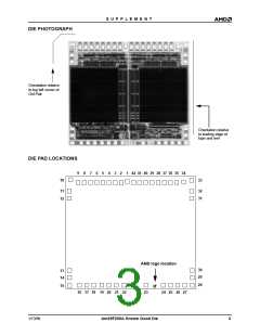
The Am29F200A in Known Good Die (KGD) form is a
2 Mbit, 5.0 Volt-only Flash memory. AMD defines KGD
as standard product in die form, tested for functionality
and speed. AMD KGD products have the same reli-
ability and quality as AMD products in packaged form.
The host system can detect whether a program or
erase operation is complete by observing the RY/BY#
pin, or by reading the DQ7 (Data# Polling) and DQ6/
DQ2 (toggle) status bits. After a program or erase
cycle has been completed, the device is ready to read
array data or accept another command.
Am29F200A Features
The Am29F200A is organized as 262,144 bytes of 8
bits each or 131,072 words of 16 bits each. The 8-bit
data appears on DQ0-DQ7; the 16-bit data appears on
DQ0-DQ15. This device is designed to be programmed
The sector erase architecture allows memory sectors
to be erased and reprogrammed without affecting the
data contents of other sectors. The device is fully
erased when shipped from the factory.
in-system with the standard system 5.0 Volt V
sup-
CC
ply. A 12.0 volt V is not required for program or erase
PP
operations.
Hardware data protection measures include a low
VCC detector that automatically inhibits write opera-
tions during power transitions. The hardware sector
protection feature disables both program and erase
operations in any combination of the sectors of mem-
ory. This can be achieved via programming equipment.
The standard Am29F200A in KGD form offers an ac-
cess time of 90 or 120 ns, allowing high-speed micro-
processors to operate without wait states. To eliminate
bus contention the device has separate chip enable
(CE#), write enable (WE#), and output enable (OE#)
controls.
The Erase Suspend feature enables the user to put
erase on hold for any period of time to read data from,
or program data to, any sector that is not selected for
erasure. True background erase can thus be achieved.
The device requires only a single 5.0 volt power sup-
ply for both read and write functions. Internally gener-
ated and regulated voltages are provided for the
program and erase operations.
The hardware RESET# pin terminates any operation
in progress and resets the internal state machine to
reading array data. The RESET# pin may be tied to the
system reset circuitry. A system reset would thus also
reset the device, enabling the system microprocessor
to read the boot-up firmware from the Flash memory.
The device is entirely command set compatible with the
JEDEC single-power-supply Flash standard. Com-
mands are written to the command register using stan-
dard microprocessor write timings. Register contents
serve as input to an internal state-machine that con-
trols the erase and programming circuitry. Write cycles
also internally latch addresses and data needed for the
programming and erase operations. Reading data out
of the device is similar to reading from other Flash or
EPROM devices.
The system can place the device into the standby mode.
Power consumption is greatly reduced in this mode.
AMD’s Flash technology combines years of Flash mem-
ory manufacturing experience to produce the highest lev-
els of quality, reliability and cost effectiveness. The device
electrically erases all bits within a sector simulta-
neously via Fowler-Nordheim tunneling. The data is
programmed using hot electron injection.
Device programming occurs by executing the program
command sequence. This initiates the Embedded
Program algorithm—an internal algorithm that auto-
matically times the program pulse widths and verifies
proper cell margin.
ELECTRICAL SPECIFICATIONS
Refer to the Am29F200A data sheet, publication
number 20380, for full electrical specifications on the
Am29F200A.
Device erasure occurs by executing the erase com-
mand sequence. This initiates the Embedded Erase
algorithm—an internal algorithm that automatically
preprograms the array (if it is not already pro-
PRODUCT SELECTOR GUIDE
Family Part Number
Am29F200A KGD
Speed Option (V
= 5.0 V ± 10%)
Max access time, ns (t
-90
90
90
35
-120
120
120
50
CC
)
ACC
Max CE# access time, ns (t
)
CE
Max OE# access time, ns (t
)
OE
2
Am29F200A Known Good Die
1/13/98

 AMD [ AMD ]