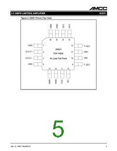
S3051
2.5 GBPS LIMITING AMPLIFIER
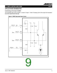
DETAILED DESCRIPTION
The referred wideband input noise (160 µVrms) al-
lows for a less than 1E-9 Bit Error Rate for inputs
down to 2 mVp-p.
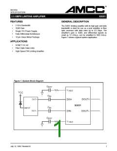
The S3051 is an integrated limiting amplifier in-
tended for high-frequency fiber-optic applications.
The circuit connects to typical transimpedance am-
plifiers found within a fiber-optic link. The linear
signal output from a transimpedance amplifier can
contain significant amounts of noise, and may vary
in amplitude over time. The S3051 limiting amplifier
quantizes the signal, and outputs a voltage limited
waveform over a 38 dB input dynamic range.
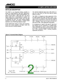
The S3051 is designed to allow adjustment of the
DC offset between the DIN+ and DIN– inputs. V+REF
can be used as a reference from which the required
offset can be subtracted to set the DC bias level at
DIN–. Similarly, V–REF can be used to set the DC
bias level at DIN+. (See Application Information).
At low signal levels, below 12 mVp-p, the circuit be-
haves as a linear amplifier. At higher levels the
device becomes a limiting amplifier.
If no adjustment is made to the input DC bias level,
two resistors can be connected in a negative feed-
back configuration in order to cancel any DC offset
at the input. This will minimize the pulse width distor-
tion. (See separate S3051 Limiting Amplifier
Application document.)
Figure 2. Functional Block Diagram
NC
VCC(OB)
7
GND(OB)
5
GND(OB)
6
8
110pF
4
5kΩ
GND(OB)
50Ω
9
V
–
REF
5kΩ
3
2
DOUT–
DOUT+
10
11
DIN–
DIN+
GS1
GS2
OB
5kΩ
5kΩ
50Ω
12
V
+
REF
1
GND(OB)
110pF
13
14
15
16
V
= +5V
CC
VCC(GS1,GS2)
GND(GS1,GS2)
VCC(GS1,SS2) GND(GS1,GS2)
NC ..... No Connect
July 14, 1999 / Revision B
2

 AMCC [ APPLIED MICRO CIRCUITS CORPORATION ]