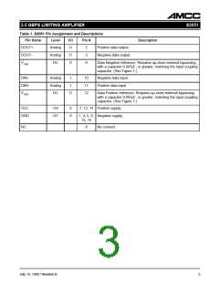
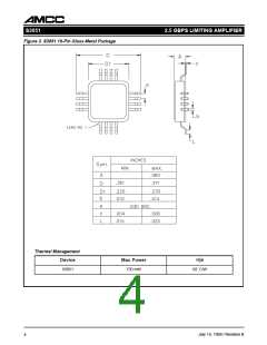
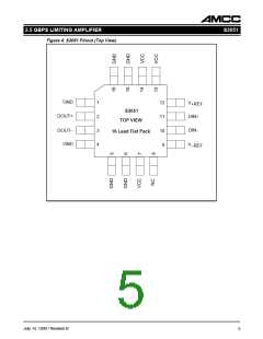
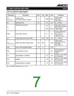
2.5 GBPS LIMITING AMPLIFIER
S3051
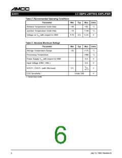
Table 4. AC Electrical Characteristics
(VCC = 5V ± 5%, TA = –40˚C to +85˚C)
Parameters
Description
Min
12
Typ
Max
Units
Conditions
Peak-to-peak,
VID =
(VIN+)-(VIN–)
Voltage Range
(Over which output is limited)
1000 mVp-p differential
(See Figure 5.)
AD
VN
Differential Gain
32
48
dB
µV
VID = 8mVp-p
Differential Input Noise
Input referred noise =
RMS output noise/low
frequency gain,
160
3.58 nV/√Hz
7 kHz–2 GHz
Input is 2.488 Gbps
223-1 PRBS, VID =
12mVp-p and
PWD
tR, tF
Pulse Width Distortion
0.1
UI
ps
1000mVp-p note 1
Output Edge Speed (20%–80%)
Differential Output Voltage Swing
100
900
165
VID = 12mVp-p
Peak-to-peak,
differential, 50Ω line
termination.
VOD
=
550
1.6
mVpp
(VOUT+)-(VOUT–
)
(See Figure 6.)
BWH
Upper Small-Signal Bandwidth
Low Frequency Cut-off
2
2
GHz
kHz
Input coupling and
bypassing as in
Figure 7.
BWL
200 kHz–2 GHz, 50Ω
line termination.
S11
S12
S22
Input Reflection Coefficient
Isolation
–15
–45
–15
dB
dB
dB
200 kHz–2 GHz, 50Ω
line termination.
200 kHz–2 GHz, 50Ω
line termination.
Output Reflection Coefficent
Note 1. Input offset calibrated out at VID = 15mV.
July 14, 1999 / Revision B
7

 AMCC [ APPLIED MICRO CIRCUITS CORPORATION ]