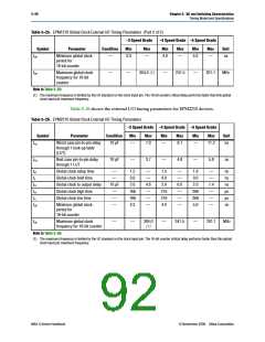
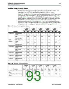
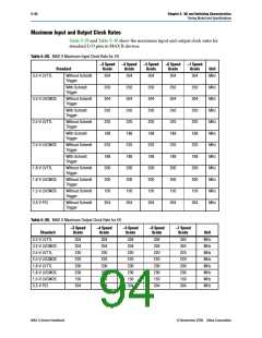
5–24
Chapter 5: DC and Switching Characteristics
Referenced Documents
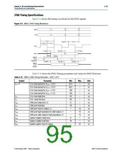
Table 5–31. MAX II JTAG Timing Parameters (Part 2 of 2)
Symbol
Parameter
Min
—
Max
25
Unit
ns
tJSZX
tJSXZ
Update register high impedance to valid output
Update register valid output to high impedance
—
25
ns
Notes to Table 5–31:
(1) Minimum clock period specified for 10 pF load on the TDOpin. Larger loads on TDOwill degrade the maximum TCK
frequency.
(2) This specification is shown for 3.3-V LVTTL/LVCMOS and 2.5-V LVTTL/LVCMOS operation of the JTAG pins. For 1.8-V
LVTTL/LVCMOS and 1.5-V LVCMOS, the tJPSU minimum is 6 ns and tJPCO, tJPZX, and tJPXZ are maximum values at 35 ns.
Referenced Documents
This chapter references the following documents:
■
I/O Structure section in the MAX II Architecture chapter in the MAX II Device
Handbook
■
Hot Socketing and Power-On Reset in MAX II Devices chapter in the MAX II Device
Handbook
■
■
■
Operating Requirements for Altera Devices Data Sheet
PowerPlay Power Analysis chapter in volume 3 of the Quartus II Handbook
Understanding and Evaluating Power in MAX II Devices chapter in the MAX II Device
Handbook
■
■
Understanding Timing in MAX II Devices chapter in the MAX II Device Handbook
Using MAX II Devices in Multi-Voltage Systems chapter in the MAX II Device
Handbook
MAX II Device Handbook
© Novermber 2008 Altera Corporation

 ALTERA [ ALTERA CORPORATION ]