3–4
Chapter 3: JTAG and In-System Programmability
In System Programmability
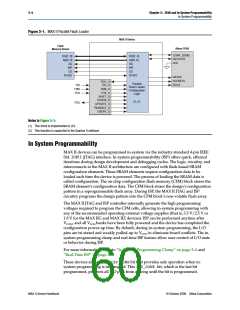
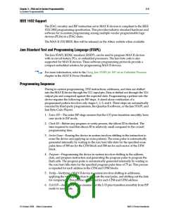
Figure 3–1. MAX II Parallel Flash Loader
MAX II Device
Flash
Memory Device
Altera FPGA
CONF_DONE
nSTATUS
nCE
DQ[7..0]
A[20..0]
OE
DQ[7..0]
A[20..0]
OE
WE
WE
CE
CE
RY/BY
RY/BY
DATA0
nCONFIG
DCLK
TDO_U
TDI_U
Parallel
TDI
TMS
TCK
Flash Loader
Configuration
Logic
TMS_U
TCK_U
SHIFT_U
CLKDR_U
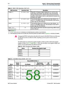
(1),(2)
TDO
UPDATE_U
RUNIDLE_U
USER1_U
Notes to Figure 3–1:
(1) This block is implemented in LEs.
(2) This function is supported in the Quartus II software.
In System Programmability
MAX II devices can be programmed in-system via the industry standard 4-pin IEEE
Std. 1149.1 (JTAG) interface. In-system programmability (ISP) offers quick, efficient
iterations during design development and debugging cycles. The logic, circuitry, and
interconnects in the MAX II architecture are configured with flash-based SRAM
configuration elements. These SRAM elements require configuration data to be
loaded each time the device is powered. The process of loading the SRAM data is
called configuration. The on-chip configuration flash memory (CFM) block stores the
SRAM element’s configuration data. The CFM block stores the design’s configuration
pattern in a reprogrammable flash array. During ISP, the MAX II JTAG and ISP
circuitry programs the design pattern into the CFM block’s non-volatile flash array.
The MAX II JTAG and ISP controller internally generate the high programming
voltages required to program the CFM cells, allowing in-system programming with
any of the recommended operating external voltage supplies (that is, 3.3 V/2.5 V or
1.8 V for the MAX IIG and MAX IIZ devices). ISP can be performed anytime after
V
CCINT and all VCCIO banks have been fully powered and the device has completed the
configuration power-up time. By default, during in-system programming, the I/O
pins are tri-stated and weakly pulled-up to VCCIO to eliminate board conflicts. The in-
system programming clamp and real-time ISP feature allow user control of I/O state
or behavior during ISP.
For more information, refer to “In-System Programming Clamp” on page 3–6 and
“Real-Time ISP” on page 3–7.
These devices also offer an ISP_DONEbit that provides safe operation when in-
system programming is interrupted. This ISP_DONE bit, which is the last bit
programmed, prevents all I/O pins from driving until the bit is programmed.
MAX II Device Handbook
© October 2008 Altera Corporation

 ALTERA [ ALTERA CORPORATION ]