Chapter 3: JTAG and In-System Programmability
3–3
IEEE Std. 1149.1 (JTAG) Boundary-Scan Support
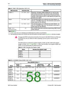
Table 3–3. 32-Bit MAX II Device IDCODE (Part 2 of 2)
Binary IDCODE (32 Bits) (1)
Version
(4 Bits)
Manufacturer
LSB
Device
Part Number
Identity (11 Bits)
(1 Bit) (2)
HEX IDCODE
0x020A50DD
0x020A60DD
EPM240Z
0000
0000
0010 0000 1010 0101
0010 0000 1010 0110
000 0110 1110
000 0110 1110
1
1
EPM570Z
Notes to Table 3–2:
(1) The most significant bit (MSB) is on the left.
(2) The IDCODE’s least significant bit (LSB) is always 1.
f
f
For JTAG AC characteristics, refer to the DC and Switching Characteristics chapter in
the MAX II Device Handbook.
For more information about JTAG BST, refer to the IEEE 1149.1 (JTAG) Boundary-Scan
Testing for MAX II Devices chapter in the MAX II Device Handbook.
JTAG Block
The MAX II JTAG block feature allows you to access the JTAG TAP and state signals
when either the USER0 or USER1instruction is issued to the JTAG TAP. The USER0
and USER1instructions bring the JTAG boundary-scan chain (TDI) through the user
logic instead of the MAX II device’s boundary-scan cells. Each USERinstruction
allows for one unique user-defined JTAG chain into the logic array.
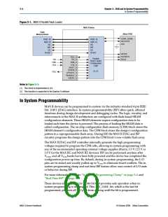
Parallel Flash Loader
The JTAG block ability to interface JTAG to non-JTAG devices is ideal for general-
purpose flash memory devices (such as Intel- or Fujitsu-based devices) that require
programming during in-circuit test. The flash memory devices can be used for FPGA
configuration or be part of system memory. In many cases, the MAX II device is
already connected to these devices as the configuration control logic between the
FPGA and the flash device. Unlike ISP-capable CPLD devices, bulk flash devices do
not have JTAG TAP pins or connections. For small flash devices, it is common to use
the serial JTAG scan chain of a connected device to program the non-JTAG flash
device. This is slow and inefficient in most cases and impractical for large parallel
flash devices. Using the MAX II device’s JTAG block as a parallel flash loader, with
the Quartus II software, to program and verify flash contents provides a fast and cost-
effective means of in-circuit programming during test. Figure 3–1 shows MAX II
being used as a parallel flash loader.
© October 2008 Altera Corporation
MAX II Device Handbook

 ALTERA [ ALTERA CORPORATION ]