2–18
Chapter 2: MAX II Architecture
User Flash Memory Block
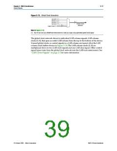
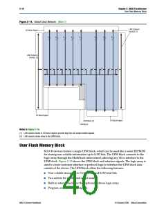
Figure 2–14. Global Clock Network (Note 1)
LAB Column
clock[3..0]
I/O Block Region
4
4
4
4
4
4
4
4
LAB Column
clock[3..0]
I/O Block Region
I/O Block Region
UFM Block (2)
CFM Block
Notes to Figure 2–14:
(1) LAB column clocks in I/O block regions provide high fan-out output enable signals.
(2) LAB column clocks drive to the UFM block.
User Flash Memory Block
MAX II devices feature a single UFM block, which can be used like a serial EEPROM
for storing non-volatile information up to 8,192 bits. The UFM block connects to the
logic array through the MultiTrack interconnect, allowing any LE to interface to the
UFM block. Figure 2–15 shows the UFM block and interface signals. The logic array is
used to create customer interface or protocol logic to interface the UFM block data
outside of the device. The UFM block offers the following features:
■
■
■
■
Non-volatile storage up to 16-bit wide and 8,192 total bits
Two sectors for partitioned sector erase
Built-in internal oscillator that optionally drives logic array
Program, erase, and busy signals
MAX II Device Handbook
© October 2008 Altera Corporation

 ALTERA [ ALTERA CORPORATION ]