2–16
Chapter 2: MAX II Architecture
Global Signals
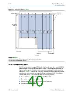
The UFM block communicates with the logic array similar to LAB-to-LAB interfaces.
The UFM block connects to row and column interconnects and has local interconnect
regions driven by row and column interconnects. This block also has DirectLink
interconnects for fast connections to and from a neighboring LAB. For more
information about the UFM interface to the logic array, see “User Flash Memory
Block” on page 2–18.
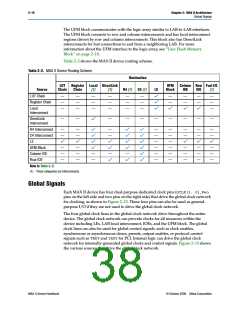
Table 2–2 shows the MAX II device routing scheme.
Table 2–2. MAX II Device Routing Scheme
Destination
LUT
Register Local DirectLink
UFM
Column Row Fast I/O
Source
LUT Chain
Chain
Chain
(1)
—
—
—
(1)
—
—
—
R4 (1)
C4 (1)
—
LE
v
v
v
Block
IOE
IOE
(1)
—
—
—
—
—
—
—
—
—
—
—
—
v
—
—
Register Chain
—
—
—
—
Local
Interconnect
—
—
v
v
DirectLink
Interconnect
—
—
v
—
—
—
—
—
—
—
—
R4 Interconnect
C4 Interconnect
LE
—
—
v
—
—
—
—
—
v
—
—
—
v
v
v
v
—
—
—
—
v
v
—
v
v
v
v
v
—
v
v
v
v
v
v
v
—
—
—
—
—
—
—
—
—
—
—
—
—
—
v
—
—
—
—
—
v
—
—
—
—
—
v
—
—
—
UFM Block
Column IOE
Row IOE
Note to Table 2–2:
(1) These categories are interconnects.
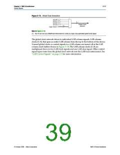
Global Signals
Each MAX II device has four dual-purpose dedicated clock pins (GCLK[3..0], two
pins on the left side and two pins on the right side) that drive the global clock network
for clocking, as shown in Figure 2–13. These four pins can also be used as general-
purpose I/O if they are not used to drive the global clock network.
The four global clock lines in the global clock network drive throughout the entire
device. The global clock network can provide clocks for all resources within the
device including LEs, LAB local interconnect, IOEs, and the UFM block. The global
clock lines can also be used for global control signals, such as clock enables,
synchronous or asynchronous clears, presets, output enables, or protocol control
signals such as TRDYand IRDYfor PCI. Internal logic can drive the global clock
network for internally-generated global clocks and control signals. Figure 2–13 shows
the various sources that drive the global clock network.
MAX II Device Handbook
© October 2008 Altera Corporation

 ALTERA [ ALTERA CORPORATION ]