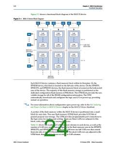
Chapter 2: MAX II Architecture
2–5
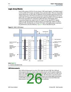
Logic Array Blocks
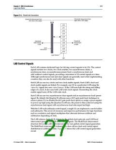
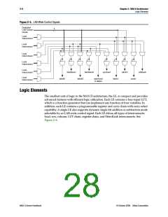
Figure 2–4. DirectLink Connection
DirectLink interconnect from
right LAB or IOE output
DirectLink interconnect from
left LAB or IOE output
LE0
LE1
LE2
LE3
LE4
LE5
LE6
LE7
LE8
LE9
DirectLink
interconnect
to right
DirectLink
interconnect
to left
Local
Interconnect
Logic Element
LAB
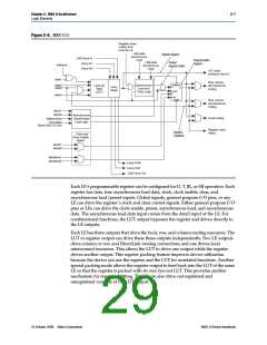
LAB Control Signals
Each LAB contains dedicated logic for driving control signals to its LEs. The control
signals include two clocks, two clock enables, two asynchronous clears, a
synchronous clear, an asynchronous preset/load, a synchronous load, and
add/subtract control signals, providing a maximum of 10 control signals at a time.
Although synchronous load and clear signals are generally used when implementing
counters, they can also be used with other functions.
Each LAB can use two clocks and two clock enable signals. Each LAB’s clock and
clock enable signals are linked. For example, any LE in a particular LAB using the
labclk1signal also uses labclkena1. If the LAB uses both the rising and falling
edges of a clock, it also uses both LAB-wide clock signals. Deasserting the clock
enable signal turns off the LAB-wide clock.
Each LAB can use two asynchronous clear signals and an asynchronous load/preset
signal. By default, the Quartus II software uses a NOTgate push-back technique to
achieve preset. If you disable the NOTgate push-back option or assign a given register
to power-up high using the Quartus II software, the preset is then achieved using the
asynchronous load signal with asynchronous load data input tied high.
With the LAB-wide addnsub control signal, a single LE can implement a one-bit adder
and subtractor. This saves LE resources and improves performance for logic functions
such as correlators and signed multipliers that alternate between addition and
subtraction depending on data.
The LAB column clocks [3..0], driven by the global clock network, and LAB local
interconnect generate the LAB-wide control signals. The MultiTrack interconnect
structure drives the LAB local interconnect for non-global control signal generation.
The MultiTrack interconnect’s inherent low skew allows clock and control signal
distribution in addition to data. Figure 2–5 shows the LAB control signal generation
circuit.
© October 2008 Altera Corporation
MAX II Device Handbook

 ALTERA [ ALTERA CORPORATION ]