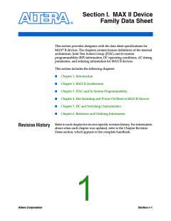
Features
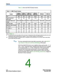
Table 1–1 shows the MAX II family features.
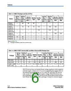
Table 1–1. MAX II Family Features
EPM240
Feature
EPM570
EPM1270
EPM2210
EPM2210G
EPM240Z
EPM570Z
EPM240G EPM570G EPM1270G
LEs
240
192
570
440
1,270
980
2,210
1,700
240
192
570
440
Typical Equivalent
Macrocells
Equivalent Macrocell
Range
128 to 240 240 to 570 570 to 1,270 1,270 to 2,210
128 to 240
240 to 570
UFM Size (bits)
Maximum User I/O pins
tPD1 (ns) (1)
8,192
80
8,192
160
5.4
8,192
212
6.2
8,192
272
7.0
8,192
80
8,192
160
9.0
4.7
7.5
f
t
t
CNT (MHz) (2)
SU (ns)
304
1.7
304
1.2
304
1.2
304
1.2
152
2.3
152
2.2
CO (ns)
4.3
4.5
4.6
4.6
6.5
6.7
Notes to Table 1–1:
(1) tPD1 represents a pin-to-pin delay for the worst case I/O placement with a full diagonal path across the device and
combinational logic implemented in a single LUT and LAB that is adjacent to the output pin.
(2) The maximum frequency is limited by the I/O standard on the clock input pin. The 16-bit counter critical delay
will run faster than this number.
f
For more information about equivalent macrocells, refer to the MAX II
Logic Element to Macrocell Conversion Methodology white paper.
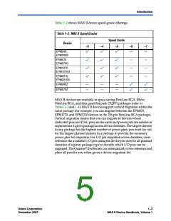
MAX II and MAX IIG devices are available in three speed grades: –3, –4,
and –5, with –3 being the fastest. Similarly, MAX IIZ devices are available
in two speed grades: –6, –7, with –6 being faster. These speed grades
represent the overall relative performance, not any specific timing
parameter. For propagation delay timing numbers within each speed
grade and density, refer to the DC and Switching Characteristics chapter in
the MAX II Device Handbook.
1–2
MAX II Device Handbook, Volume 1
Core Version a.b.c variable
Altera Corporation
December 2007

 ALTERA [ ALTERA CORPORATION ]