Timing Model
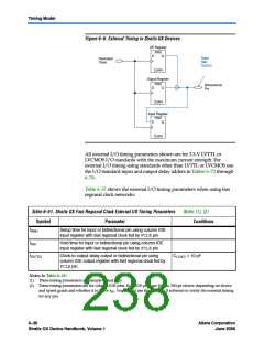
Figure 6–6. External Timing in Stratix GX Devices
OE Register
PRN
D
Q
t
t
t
INSU
INH
Dedicated
Clock
OUTCO
CLRN
Output Register
PRN
Bidirectional
Pin
D
Q
CLRN
Input Register
PRN
D
Q
CLRN
All external I/O timing parameters shown are for 3.3-V LVTTL or
LVCMOS I/O standards with the maximum current strength. For
external I/O timing using standards other than LVTTL or LVCMOS use
the I/O standard input and output delay adders in Tables 6–72 through
6–76.
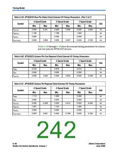
Table 6–51 shows the external I/O timing parameters when using fast
regional clock networks.
Table 6–51. Stratix GX Fast Regional Clock External I/O Timing Parameters
Notes (1), (2)
Conditions
Symbol
Parameter
tINSU
Setup time for input or bidirectional pin using column IOE
input register with fast regional clock fed by FCLKpin
tINH
Hold time for input or bidirectional pin using column IOE
input register with fast regional clock fed by FCLKpin
tOUTCO
Clock-to-output delay output or bidirectional pin using
column IOE output register with fast regional clock fed by
FCLKpin
CLOAD = 10 pF
Notes to Table 6–51:
(1) These timing parameters are sample-tested only.
(2) These timing parameters are for column IOE pins. Row IOE pins are 100- to 250-ps slower depending on device
and speed grade and whether it is tCO or tSU. You should use the Quartus II software to verify the external timing
for any pin.
6–36
Altera Corporation
June 2006
Stratix GX Device Handbook, Volume 1

 ALTERA [ ALTERA CORPORATION ]