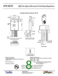
Off-Line Quasi-Resonant Switching Regulators
STR-X6757
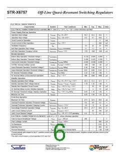
ELECTRICAL CHARACTERISTICS
Characteristic
Symbol
Test Conditions
Min.
Typ.
Max.
Units
ELECTRICAL CHARACTERISTICS for Controller (MIC)1, valid at TA = 25°C, VCC = 20 V, unless otherwise specified
Power Supply Start-up Operation
VCC = 0→20 V
Operation Start Voltage
VCC(ON)
VCC(OFF)
ICC(ON)
16.3
8.8
–
18.2
9.7
–
19.9
10.6
6
V
V
VCC = 20→8.8 V
Operation Stop Voltage
Circuit Current In Operation
mA
μA
kHz
V
VCC = 15 V
Circuit Current In Non-Operation
Oscillation Frequency
ICC(OFF)
fosc
VSSOLP(SS)
ISSOLP(SS)
–
–
100
25
19
22
VSS/OLP increasing
VSS/OLP = 0 V
Soft Start Operation Stop Voltage
Soft Start Operation Charging Current
Normal Operation
1.1
–710
1.2
–550
1.4
–390
μA
Bottom-Skip Operation Threshold Voltage 1
Bottom-Skip Operation Threshold Voltage 2
Overcurrent Detection Threshold Voltage
OCP/BD Terminal Outflow Current
Quasi-Resonant Operation Threshold Voltage 1
Quasi-Resonant Operation Threshold Voltage 2
FB Terminal Threshold Voltage
VOCPBD(BS1)
VOCPBD(BS2)
VOCPBD(LIM)
IOCPBD
–0.720 –0.665 –0.605
–0.485 –0.435 –0.385
–0.995 –0.940 –0.895
V
V
VOCP/BD falling
VOCP/BD = –0.95 V
VOCP/BD falling
VOCP/BD rising
VFB rising
V
–250
0.28
0.67
1.32
600
–100
0.40
0.80
1.45
1000
–40
0.52
0.93
1.58
1400
μA
V
VOCPBD(TH1)
VOCPBD(TH2)
VFB(OFF)
V
V
VFB = 1.6 V
FB Terminal Inflow Current (Normal Operation)
Standby Operation
IFB(ON)
μA
VCC = 0→15 V, VFB = 1.6 V
VCC(SK) = VCC(S) – VCC(OFF)
VCC = 10.2 V, VFB = 1.6 V
VCC = 10.2 V, VFB = 1.6 V
VCC = 15 V, VFB rising
Standby Operation Start Voltage
Standby Operation Start Voltage Interval
Standby Non-Operation Circuit Current
FB Terminal Inflow Current, Standby Operation
FB Terminal Threshold Voltage, Standby Operation
Minimum On Time
VCC(S)
VCC(SK)
ICC(S)
10.3
1.10
–
11.2
1.35
20
12.1
1.65
56
V
V
μA
μA
V
IFB(S)
–
4
14
VFB(S)
tON(MIN)
0.55
0.65
1.10
1.00
1.50
1.35
μs
Protection Operation
Maximum On Time
tON(MAX)
VSSOLP(OLP)
ISSOLP(OLP)
VCC(OVP)
ICC(H)
27.5
4.0
–16
25.5
–
32.5
4.9
39.0
5.8
μs
V
Overload Protection Operation Threshold Voltage
Overload Protection Operation Charging Current
Overvoltage Protection Operation Voltage
Latch Circuit Holding Current2
VSS/OLP = 2.5 V
–11
27.7
45
–6
μA
V
VCC = 0→30 V
29.9
140
8.5
VCC(OFF)– 0.3 V
μA
V
Latch Circuit Release Voltage2
VCC(La.OFF)
6.0
7.2
VCC = 30→6 V, OVP operating
ELECTRICAL CHARACTERISTICS for MOSFET, valid at TA = 25°C, unless otherwise specified
Drain-to-Source Breakdown Voltage
Drain Leakage Current
On Resistance
VDSS
IDSS
RDS(on)
tf
IDSS = 300 μA
VDSSS = 650 V
IDS = 3.4 A
650
–
–
–
–
–
–
–
V
μA
300
0.62
500
1.09
–
Ω
Switching Time
–
ns
Thermal Resistance
Rθch-F
Channel to internal frame
–
°C/W
1Current polarity with respect to the IC: positive current indicates current sink at the terminal named, negative current indicates source at the
terminal named.
2The latch circuit means a circuit operated OVP and OLP.
Allegro MicroSystems, Inc.
115 Northeast Cutoff
6
Worcester, Massachusetts 01615-0036 U.S.A.
1.508.853.5000; www.allegromicro.com

 ALLEGRO [ ALLEGRO MICROSYSTEMS ]