Hall Effect Linear Current Sensor with Overcurrent
Fault Output for < 100 V Isolation Applications
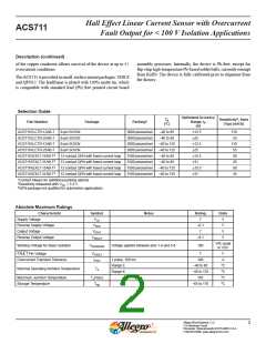
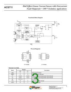
ACS711
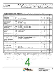
COMMON OPERATING CHARACTERISTICS over full range of TA and VCC = 3.3 V, unless otherwise specified
Characteristic
Symbol
Test Conditions
Min.
Typ.
Max.
Units
ELECTRICAL CHARACTERISTICS
Supply Voltage1
VCC
3
–
3.3
4
5.5
5.5
1
V
mA
nF
kꢀ
mꢀ
mꢀ
μs
Supply Current
ICC
VCC = 3.3 V, output open
Output Capacitance Load
Output Resistive Load
CLOAD
RLOAD
VIOUT to GND
–
–
VIOUT to GND
15
–
–
–
EX package, TA = 25°C
LC package, TA = 25°C
IP = IPMAX, TA = 25°C, COUT = open
IP = IP(max), TA = 25°C, COUT = open
0.6
1.2
3.5
1.2
4.6
100
±1
100
–
Primary Conductor
Resistance
RIP
–
–
VIOUT Rise Time
Propagation Delay Time
Response Time
Internal Bandwidth2
Nonlinearity
tr
–
–
tPROP
–
–
ꢁs
tRESPONSE IP = IP(max), TA = 25°C, COUT = open
–
–
ꢁs
BWI
ELIN
–3 dB, TA = 25°C
Over full range of IP
Apply full scale IP
–
–
kHz
%
–
–
Symmetry
ESYM
–
–
%
VCC
0.3
–
VIOH
–
–
V
VIOUT Saturation Voltages
VIOL
–
–
–
0.3
–
V
V
Quiescent Output Voltage
Power-On Time
VIOUT(Q)
IP = 0 A, TA = 25°C
VCC / 2
Output reaches 90% of steady-state level, TA = 25°C,
20 A present on primary conductor
tPO
–
35
–
μs
¯¯¯¯¯¯¯¯¯
FAULT Pin Characteristics
¯¯¯¯¯¯¯¯¯
FAULT Operating Point
IFAULT
RPU
–
1
± 1 x IP
–
–
–
A
¯¯¯¯¯¯¯¯¯
FAULT Output Pullup
kΩ
Resistor
VCC
–
VOH
–
–
V
0.3
0.3
1.3
¯¯¯¯¯¯¯¯¯
FAULT Output Voltage
VOL
RPU = 1 kΩ
–
–
–
–
V
¯¯¯¯¯¯¯¯¯
FAULT Response Time
tFAULT
Measured from | IP | > | IFAULT | to VFAULT ≤ VOL
ꢁs
V
CC Off Voltage Level for
VCCFR
tCCFR
–
–
–
200
–
mV
Fault Reset3
V
CC Off Duration for
100
ꢁs
Fault Reset3
1Devices are programmed for maximum accuracy at 3.3 V VCC levels. The device contains ratiometry circuits that accurately alter the 0 A Output
Voltage and Sensitivity level of the device in proportion to the applied VCC level. However, as a result of minor nonlinearities in the ratiometry circuit
additional output error will result when VCC varies from the 3.3 V VCC level. Customers that plan to operate the device from a 5 V regulated supply
should contact their local Allegro sales representative regarding expected device accuracy levels under these bias conditions.
2Calculated using the formula BWI = 0.35 / tr.
3
¯¯¯¯¯¯¯¯¯
After the FAULT pin is latched low, the only way to reset it is through a power-off and power-on cycle on the VCC pin. For fault reset, VCC must stay
below VCCFR for a period greater than tCCFR before settling to the normal operation voltage (3 to 5.5 V).
Allegro MicroSystems, LLC
115 Northeast Cutoff
4
Worcester, Massachusetts 01615-0036 U.S.A.
1.508.853.5000; www.allegromicro.com

 ALLEGRO [ ALLEGRO MICROSYSTEMS ]