Hall Effect Linear Current Sensor with Overcurrent
Fault Output for < 100 V Isolation Applications
ACS711
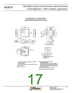
Package EX, 12-Contact QFN
With Fused Sensed Current Loop
0.30
3.00 BSC
12
0.85
1.27
12
MIN
1
1
2
A
3.00 BSC
2.90
1.00
0.80
MIN
Branded Face
0.50
D
C
9X
0.70
SEATING
0.08
C
PLANE
2.05 REF
2.70
0.50 BSC
0.25
0.75 ±0.05
C
PCB Layout Reference View
+0.05
–0.07
1
NNNN
YYWW
LLLL
0.40±0.10
B
0.20
1.79
2
1
Standard Branding Reference View
E
N = Device part number
12
Y = Last two digits of year of manufacture
W = Week of manufacture
L = Lot number
C
Reference land pattern layout (reference IPC7351
QFN50P300X300X80-17W4M);
For reference only, not for tooling use (reference JEDEC MO-220WEED
except for fused current path)
All pads a minimum of 0.20 mm from all adjacent pads; adjust as
necessary to meet application process requirements and PCB layout
tolerances; when mounting on a multilayer PCB, thermal vias at the
exposed thermal pad land can improve thermal dissipation (reference
EIA/JEDEC Standard JESD51-5)
Dimensions in millimeters
Exact case and lead configuration at supplier discretion within limits shown
A
Terminal #1 mark area
B
Fused sensed current path
D
E
Coplanarity includes exposed current path and terminals
Branding scale and appearance at supplier discretion
Allegro MicroSystems, LLC
115 Northeast Cutoff
17
Worcester, Massachusetts 01615-0036 U.S.A.
1.508.853.5000; www.allegromicro.com

 ALLEGRO [ ALLEGRO MICROSYSTEMS ]