Hall Effect Linear Current Sensor with Overcurrent
Fault Output for < 100 V Isolation Applications
ACS711
Application Information
should be connected using the arrangement of vias
shown below.
Layout
To optimize thermal and electrical performance, the
following features should be included in the printed
circuit board:
• The two solder pads at the ends of the exposed pad
loop should be placed directly on the copper trace
that conducts the primary current.
• The primary leads should be connected to as much
copper area as is available.
• When using vias under exposed pads, such as with
the EX package, using plugged vias prevents wicking
of the solder from the pad into the via during reflow.
Whether or not to use plugged vias should be evalu-
ated in the application.
• The copper should be 2 oz. or heavier.
• Additional layers of the board should be used for
conducting the primary current if possible, and
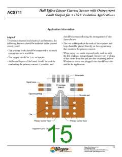
Solder pads
Signal traces
EX package
footprint
Exposed pad loop
Via under pad
Via
Primary Current Trace
Primary Current Trace
Suggested Layout. EX package shown.
Allegro MicroSystems, LLC
115 Northeast Cutoff
15
Worcester, Massachusetts 01615-0036 U.S.A.
1.508.853.5000; www.allegromicro.com

 ALLEGRO [ ALLEGRO MICROSYSTEMS ]