Isolated, Digital Output, Power Monitoring IC
with Zero-Crossing Detection, Overcurrent and Overvoltage Flagging
ACS37800
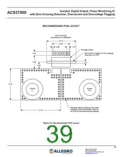
RECOMMENDED PCB LAYOUT
NOT TO SCALE
All dimensions in millimeters.
15.75
9.54
1.27
0.65
Package Outline
Slot in PCB to maintain >8 mm creepage
once part is on PCB
2.25
7.25
1.27
3.56
17.27
Current
In
Current
Out
Perimeter holes for stitching to the other,
matching current trace design, layers of
the PCB for enhanced thermal capability.
21.51
Figure 34: Recommended PCB Layout
39
Allegro MicroSystems
955 Perimeter Road
Manchester, NH 03103-3353 U.S.A.
www.allegromicro.com

 ALLEGRO [ ALLEGRO MICROSYSTEMS ]