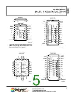
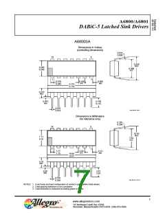
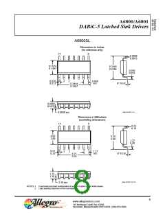
A6800/A6801
DABiC-5 Latched Sink Drivers
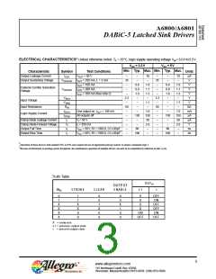
ELECTRICAL CHARACTERISTICS1 Unless otherwise noted: TA = 25°C, logic supply operating voltage Vdd =3.0Vto5.5V
V
dd = 3.3V
Vdd = 5V
Min. Typ. Max. Min. Typ. Max.
Characteristic
Output Leakage Current
Output Sustaining Voltage
Symbol
Test Conditions
Units
µA
V
ICEX
VOUT = 50 V
–
35
–
–
–
10
–
–
35
–
–
–
10
–
VCE(SUS) IOUT = 350 mA, L = 3 mH
IOUT = 100 mA
0.8
0.9
1.0
–
1.0
1.1
1.3
–
0.8
0.9
1.0
–
1.0
1.1
1.3
–
V
Collector-Emitter Saturation
Voltage
VCE(SAT) IOUT = 200 mA
–
–
V
IOUT = 350 mA (See note 2)
–
–
V
VIN(1)
VIN(0)
RIN
2.2
–
3.3
–
V
Input Voltage
–
1.1
–
–
1.7
–
V
Input Resistance
Logic Supply Current
50
–
–
50
–
–
kΩ
mA
µA
µA
V
IDD(1)
One output on, IOUT = 100 mA
All outputs off
–
1.0
150
50
2.0
–
–
1.0
150
50
2.0
–
IDD(0)
–
130
–
–
130
–
Clamp Diode Leakage Current
Clamp Diode Forward Voltage
Output Fall Time
Ir
Vf
tf
Vr= 50 V
–
–
If = 350 mA
–
–
–
–
VCC = 50V, R1 = 500 Ω, C1≤30pF
VCC = 50V, R1 = 500 Ω, C1≤30pF
–
80
100
–
80
100
ns
ns
Output Rise Time
tr
–
–
–
–
1
2
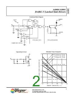
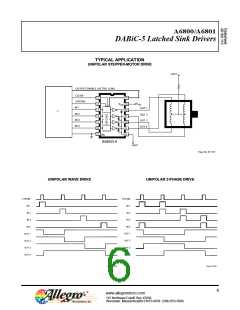
Operation of these devices with standard TTL or DTL may require the use of appropriate pull-up resistors to ensure a minimum logic 1.
Because of limitations on package power dissipation, the simultaneous operation of multiple drivers can only be accomplished by reduction in duty cycle.
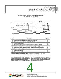
Truth Table
OUT
N
OUTPUT
E NAB LE
IN
S TR OB E
C LE AR
t-1
t
N
0
1
X
X
X
X
1
1
X
X
0
0
0
0
1
X
0
0
0
0
X
1
0
0
X
X
OFF
ON
X
OFF
OFF
ON
X
ON
OFF
OFF
X
= irrelevant
t-1 = previous output s tate
= present output state
t
3
www.allegromicro.com
115 Northeast Cutoff, Box 15036
Worcester, Massachusetts 01615-0036 (508) 853-5000

 ALLEGRO [ ALLEGRO MICROSYSTEMS ]