A3425
Ultra-Sensitive Dual-Channel Quadrature Hall-Effect Bipolar Switch
Functional Description
Chopper-Stabilized Technique
When using Hall effect technology, a limiting factor
chop frequency. This high-frequency operation allows
for a greater sampling rate, which produces higher
accuracy and faster signal processing capability. This
approach desensitizes the chip to the effects of ther-
mal and mechanical stress. The disadvantage to this
approach is that jitter, also known as 360° repeatability,
can be induced on the output signal. The sample-and-
hold process, used by the demodulator to store and
recover the signal, can slightly degrade the signal-to-
noise ratio. This is because the process generates rep-
licas of the noise spectrum at the baseband, causing a
decrease in jitter performance. However, the improve-
ment in switchpoint performance, resulting from the
reduction of the effects of thermal and mechanical
stress, outweighs the degradation in the signal-to-noise
ratio.
for switchpoint accuracy is the small signal voltage
developed across the Hall element. This voltage is
disproportionally small relative to the offset that can
be produced at the output of the Hall device. This
makes it difficult to process the signal and maintain
an accurate, reliable output over the specified tem-
perature and voltage range.
Chopper stabilization is a unique approach used
to minimize Hall offset on the chip. The patented
Allegro technique, dynamic quadrature offset can-
cellation, removes key sources of the output drift
induced by thermal and mechanical stress. This offset
reduction technique is based on a signal modulation-
demodulation process. The undesired offset signal is
separated from the magnetically induced signal in the
frequency domain through modulation. The subse-
quent demodulation acts as a modulation process for
the offset, causing the magnetically-induced signal to
recover its original spectrum at the baseband level,
while the dc offset becomes a high-frequency signal.
Then, using a low-pass filter, the signal passes while
the modulated dc offset is suppressed.
This technique produces devices that have an
extremely stable quiescent Hall element output volt-
age, are immune to thermal stress, and have precise
recoverability after temperature cycling. This tech-
nique is made possible through the use of a BiCMOS
process, which allows the use of low-offset and
low-noise amplifiers in combination with high-density
logic integration and sample-and-hold circuits. This
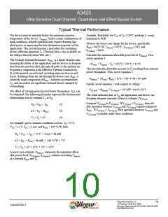
process is illustrated in the following diagram.
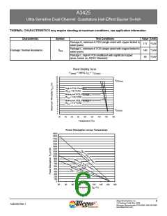
The chopper stabilization technique uses a 170 kHz
high-frequency clock. The Hall element chopping
occurs on each clock edge, resulting in a 340 kHz
Regulator
Low-
Pass
Filter
Amp
Chopper stabilization circuit (dynamic quadrature offset cancellation)
Allegro MicroSystems, Inc.
115 Northeast Cutoff, Box 15036
Worcester, Massachusetts 01615-0036 (508) 853-5000
www.allegromicro.com
7
A3425DS-Rev. !

 ALLEGRO [ ALLEGRO MICROSYSTEMS ]