A3425
Ultra-Sensitive Dual-Channel Quadrature Hall-Effect Bipolar Switch
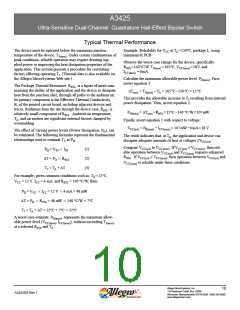
THERMAL CHARACTERISTICS may require derating at maximum conditions, see application information
Characteristic
Symbol
Test Conditions
Value Units
Package K, minimum-K PCB (single-sided with copper limited to
solder pads)
177 ºC/W
Package L, minimum-K PCB (single-sided with copper limited to
solder pads)
RθJA
Package Thermal Resistance
140 ºC/W
Package L, high-K PCB (multilayer with significant copper
areas, based on JEDEC standard)
80
ºC/W
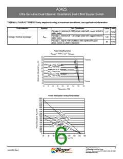
Power Derating Curve
TJ(max) = 165ºC; ICC = ICC(max)
20
19
18
17
16
15
14
13
12
11
10
9
V
CC(max)
High-K PCB, Package L
(RθJA = 80 ºC/W)
Minimum-K PCB, Package L
(RθJA = 140 ºC/W)
Minimum-K PCB, Package K
(RθJA = 177 ºC/W)
8
7
6
5
4
3
V
CC(min)
2
20
40
60
80
100
120
140
160
180
Temperature (ºC)
Power Dissipation versus Temperature
1900
1800
1700
1600
1500
1400
1300
1200
1100
1000
900
800
700
600
500
400
300
200
100
0
20
40
60
80
100
120
140
160
180
Temperature, T (°C)
A
Allegro MicroSystems, Inc.
6
115 Northeast Cutoff, Box 15036
A3425DS-Rev. !
Worcester, Massachusetts 01615-0036 (508) 853-5000
www.allegromicro.com

 ALLEGRO [ ALLEGRO MICROSYSTEMS ]