[AK4679]
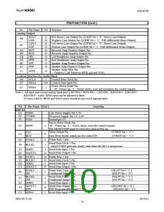
PIN/FUNCTION (Cont.)
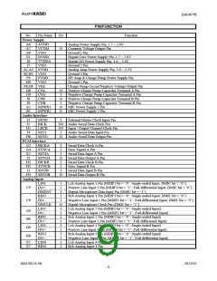
Function
No.
Pin Name
I/O
Analog Output
ROUT
LON
LOUT
LOP
RCP
RCN
HPL
HPR
SPP
O
O
O
O
O
O
O
O
O
O
Rch Stereo Line Output Pin (LODIF bit = “0”: Stereo Line Output)
Negative Line Output Pin (LODIF bit = “1”: Full-differential Mono Output)
Lch Stereo Line Output Pin (LODIF bit = “0”: Stereo Line Output)
Positive Line Output Pin (LODIF bit = “1”: Full-differential Mono Output)
Receiver-Amp Positive Output Pin
Receiver-Amp Negative Output Pin
Lch Headphone-Amp Output Pin
Rch Headphone-Amp Output Pin
B6
B7
A4
B4
E8
E9
B1
A2
Speaker-Amp Positive Output Pin
Speaker-Amp Negative Output Pin
SPN
Speaker-Amp Filter Pin
C1
SPFIL
O
Connect 2.2nF between SPFIL pin and VSS1.
Control Interface for Audio Block
G6
H7
SCLA
SDAA
I
Control Data Clock Pin
I/O Control Data Input Pin
Power-Down Mode Pin
“H”: Power-up, “L”: Power-down, reset and initializes the control register.
G7
PDNA
I
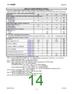
Note 1. All input pins except analog input pins (LIN1/IN1+, RIN1/IN1−, LIN2/IN2-, RIN2/IN2+, LIN3/IN3+,
RIN3/IN3−, LIN4, RIN4) must not be allowed to float.
I/O pins (LRCK, BICK and SDAA pins) should be processed appropriately.
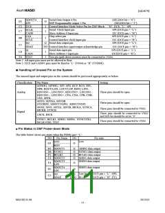
NO
Pin Name I/O
Function
DSP I/O
G1 VDDE
D1 TVDDE
F1 VSS4
-
-
-
Core Power Supply Pin 1.2V
I/O power Supply Pin 1.6∼3.6V
Ground pin 0V
Power-Down Mode Pin
D7 PDNE
I
“H”: Power-up, “L”: Power-down, reset the control register.
The AK4679 DSP must be reset once upon power-up.
Status Output Pin
(STRDY bit = “0”)
(STRDY bit = “1”)
STO
G3
O
Data Write Ready output pin for control I/F
Frame Sync 1 pin
RDY
G5 SYNC1
I
I
Serial Data Clock 1 Pin
AK4679 DSP goes into stanby state when BCLK1 is not present.
Serial Data Input 1 Pin
F6 BCLK1
F5 SDIN1
I
Serial Data Output 1 Pin
H1 SDOUT1
O
Frame Sync 1 pin
D6 SYNC2
F2 BCLK2
D3 SDIN2
C4 SDOUT2
O
O
I
Serial Data Clock 2 Pin
Serial Data Input 2 Pin
Serial Data Output 2 Pin
O
SYNC3
JX1
BCLK3
JX0
Frame Sync 3 pin
(SELPT bit = “1”)
D5
I
Conditional Jump 1 Pin
Serial Data Clock 3 Pin
Conditional Jump 0 Pin
Serial Data Input 3 Pin
Serial Data Output 3 Pin
DSP Programmable output 0 Pin
Serial Data Input 4 Pin
(SELPT bit = “0”)
(SELPT bit = “1”)
(SELPT bit = “0”)
F3
I
I
E3 SDIN3
SDOUT3
GP0
C3 SDIN4
(SELDO3 bit = “0”)
(SELDO3 bit = “1”)
F4
O
I
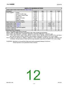
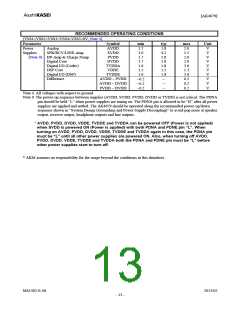
MS1402-E-06
2013/02
- 10 -

 AKM [ ASAHI KASEI MICROSYSTEMS ]