[AK4679]
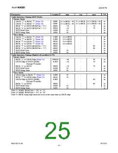
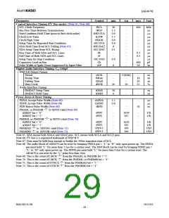
Parameter
Symbol
min
typ
max
Unit
Control Interface Timing (I2C Bus mode): (Note 65, Note 66)
SCL Clock Frequency
fSCL
tBUF
30
1.3
0.6
1.3
0.6
0.6
0
0.1
-
-
-
-
-
-
-
-
-
-
-
-
-
-
-
400
-
-
-
-
-
-
-
0.3
0.3
-
400
50
kHz
μs
μs
μs
μs
μs
μs
μs
μs
μs
μs
pF
ns
Bus Free Time Between Transmissions
Start Condition Hold Time (prior to first clock pulse)
Clock Low Time
tHD:STA
tLOW
tHIGH
tSU:STA
tHD:DAT
tSU:DAT
tR
Clock High Time
Setup Time for Repeated Start Condition
SDA Hold Time from SCL Falling (Note 67)
SDA Setup Time from SCL Rising
Rise Time of Both SDA and SCL Lines
Fall Time of Both SDA and SCL Lines
Setup Time for Stop Condition
tF
tSU:STO
Cb
0.6
-
0
Capacitive Load on Bus
Pulse Width of Spike Noise Suppressed by Input Filter
tSP
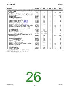
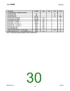
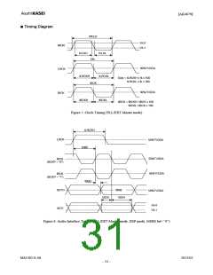
Digital Audio Interface Timing: CL=100pF
DMCLK Output Timing
Period
tSCK
tSRise
tSFall
dSCK
-
-
-
1/(64fs)
-
ns
ns
ns
%
Rising Time
Falling Time
Duty Cycle
-
-
50
10
10
55
45
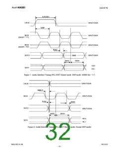
Audio Interface Timing
DMDAT Setup Time
DMDAT Hold Time
tDMS
tDMH
50
0
-
-
-
-
ns
ns
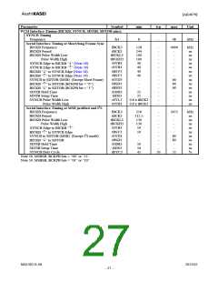
Power-down & Reset Timing
PDNA Accept Pulse Width (Note 68)
PDNE Accept Pulse Width (Note 68)
PDN Reject Pulse Width (Note 68)
PMADL or PMADR “↑” to SDTO valid (Note 69)
ADRST bit = “0”
tAPDA
tAPDE
tRPD
1.5
0.6
-
-
-
-
μs
μs
ns
50
tPDV
tPDV
-
-
1059
267
-
-
1/fs
1/fs
ADRST bit = “1”
PMDML or PMDMR “↑” to SDTO valid (Note 70)
ADRST bit = “0”
ADRST bit = “1”
PMSRAO “↑” to SDTOA valid (Note 71)
PMSRBO “↑” to SDTOB valid (Note 72)
tPDV
tPDV
tPDV2
tPDV3
-
-
-
-
1059
267
164
164
-
-
1/fs
1/fs
1/fs2
1/fs3
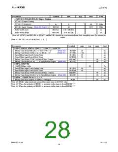
Note 65. SDA means both SDAA and SDAE pins. SCL means both SCLA and SCLE pins.
Note 66. I2C-bus is a registered trademark of NXP B.V.
Note 67. Data must be held long enough to bridge the 300ns-transition time of SCL.
Note 68. The audio block of AK4679 can be reset by bringing PDNA pin = “L” to “H” only upon power up. The PDNA
pin must held “L” for more than 1.5μs for a certain reset. The DSP block can be reset by bringing PDNE pin =
“L” to “H” only upon power up. The PDNE pin must held “L” for more than 0.6μs for a certain reset. The
AK4679 is not reset by the “L” pulse less than 50ns.
Note 69. This is the count of LRCK “↑” from the PMADL or PMADR bit = “1”.
Note 70. This is the count of LRCK “↑” from the PMDML or PMDMR bit = “1”.
Note 71. This is the count of SYNCA “↑” from the PMSRAO bit = “1”.
Note 72. This is the count of SYNCB “↑” from the PMSRBO bit = “1”.
MS1402-E-06
2013/02
- 29 -

 AKM [ ASAHI KASEI MICROSYSTEMS ]