[AK4679]
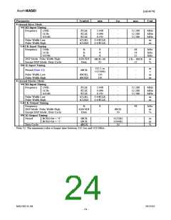
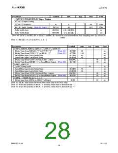
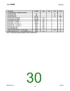
Parameter
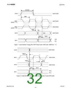
SYNC1/3, BCLK1/BCLK3 Input Timing
Symbol
min
typ
max
Unit
SYNC1/3 Input Timing
SYNC1/3 frequency
fs
8
48
kHz
kHz
ns
BCLK1 Input Timing (Note 60, Note 61)
Pulse width Low
fBCLK
tBCKL1
tBCKH1
64
3072
0.4 x tBCLK
0.4x tBCLK
Pulse width High
ns
Note 60. SYNC1 and BCLK1 or SYNC3 and BCLK3 should be synchronized and their sampling rates (fs) should be
stable
Note 61. fBCLK ≥ 4 x N x fs (N=1, 2, 3….)
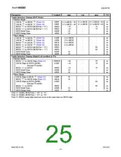
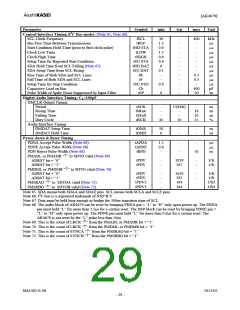
Parameter
Symbol
min
typ
max
Unit
SDIN1, SDIN3, SDIN4, SDOUT1, SDOUT3, SDOUT4
Delay Time from BICLK1 “↑” to SYNC1 “↑”
Delay Time from SYNC1 “↓” to BICK1 “↑”
Serial Data Input Latch Setup Time
Serial Data Input Latch Hold Time
Delay Time from SYNC1 to Serial Data Output
(Note 62)
(Note 62)
tBSYD
tSYBD
tB1IDS
tB1IDH
tSY1OD
tB1OD
20
100
40
ns
ns
ns
ns
ns
ns
40
40
40
Delay Time from BICK1 “↓” to Serial Data Output (Note 63)
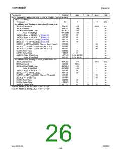
SDIN2, SDOUT2
SYNC2 Duty cycle
Serial Data Input Latch Setup Time
Serial Data Input Latch Hold Time
Delay Time from SYNC2 to Serial Data Outputs
Delay Time from BCLK2 “↓”to Serial Data Output (Note 64)
SDINn → SDOUTn (n=1, 2, 3, 4)
50
%
ns
ns
ns
ns
tB2IDS
tB2IDH
tSY2OD
tB2OD
40
40
40
40
Delay time from SDINn to SDOUTn Output
tIOD
60
ns
Note 62. BICK1 edge must not occur at the same time as SYNC1 edge.
Note 63. When the polarity of BICK1 is inverted, delay time is from BICK1 “↑”.
Note 64. When the polarity of BICK2 is inverted, delay time is from BICK2 “↑”
MS1402-E-06
2013/02
- 28 -

 AKM [ ASAHI KASEI MICROSYSTEMS ]