[AK4679]
D0
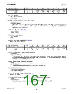
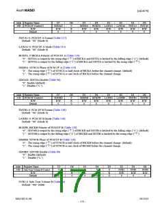
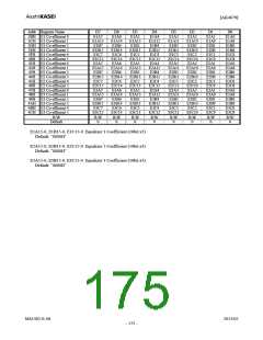
Addr Register Name
D7
SDOAD
R/W
0
D6
0
R
0
D5
MSBSA
R/W
0
D4
BCKPA
R/W
0
D3
D2
D1
20H
PCM I/F Control 0
R/W
LAWA1 LAWA0 FMTA1 FMTA0
R/W
0
R/W
0
R/W
0
R/W
0
Default
FMTA1-0: PCM I/F A Format (Table 117)
Default: “00” (Mode 0)
LAWA1-0: PCM I/F A Mode (Table 115)
Default: “00” (Mode 0)
BCKPA: P BICKA Polarity of PCM I/F A (Table 119)
“0”: SDTOA is output by the rising edge (“↑”) of BICKA and SDTIA is latched by the falling edge (“↓”). (default)
“1”: SDTOA is output by the falling edge (“↓”) of BICKA and SDTIA is latched by the rising edge (“↑”).
MSBSA: SYNCA Phase of PCM I/F A (Table 119)
“0”: The rising edge (“↑”) of SYNCA is half clock of BICKA before the channel change. (default)
“1”: The rising edge (“↑”) of SYNCA is one clock of BICKA before the channel change.
SDOAD: SDTOA Disable (Table 96)
“0”: Enable (default)
“1”: Disable (“L”)
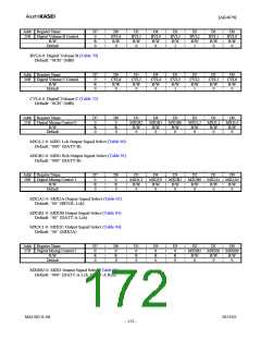
Addr Register Name
D7
SDOBD
R/W
0
D6
0
R
0
D5
MSBSB
R/W
0
D4
BCKPB
R/W
0
D3
D2
D1
D0
21H
PCM I/F Control 1
R/W
LAWB1 LAWB0 FMTB1 FMTB0
R/W
0
R/W
0
R/W
0
R/W
0
Default
FMTB1-0: PCM I/F B Format (Table 118)
Default: “00” (Mode 0)
LAWB1-0: PCM I/F B Mode (Table 116)
Default: “00” (Mode 0)
BCKPB: BICKB Polarity of PCM I/F B (Table 120)
“0”: SDTOB is output by the rising edge (“↑”) of BICKB and SDTIB is latched by the falling edge (“↓”). (default)
“1”: SDTOB is output by the falling edge (“↓”) of BICKB and SDTIB is latched by the rising edge (“↑”).
MSBSB: SYNCB Phase of PCM I/F B (Table 120)
“0”: The rising edge (“↑”) of SYNCB is half clock of BICKB before the channel change. (default)
“1”: The rising edge (“↑”) of SYNCB is one clock of BICKB before the channel change.
SDOBD: SDTOB Disable (Table 98)
“0”: Enable (default)
“1”: Disable (“L”)
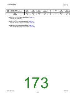
Addr Register Name
Side Tone Volume B Control
D7
0
R
0
D6
0
R
0
D5
0
R
0
D4
0
R
0
D3
0
R
0
D2
SVB2
R/W
0
D1
SVB1
R/W
0
D0
SVB0
R/W
0
22H
R/W
Default
SVB2-0: Side Tone Volume B (Table 74)
Default: “0H” (0dB)
MS1402-E-06
2013/02
- 171 -

 AKM [ ASAHI KASEI MICROSYSTEMS ]