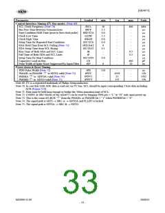
[AK4675]
Parameter
Symbol
min
typ
max
Units
Control Interface Timing (I2C Bus mode): (Note 69)
SCL Clock Frequency (Note 70)
fSCL
tBUF
30
1.3
0.6
1.3
0.6
0.6
0
0.1
-
-
-
-
-
-
-
-
-
-
-
-
-
-
-
400
-
-
-
-
-
-
-
0.3
0.3
-
400
50
kHz
μs
μs
μs
μs
μs
μs
μs
μs
μs
μs
pF
ns
Bus Free Time Between Transmissions
Start Condition Hold Time (prior to first clock pulse)
Clock Low Time
tHD:STA
tLOW
tHIGH
tSU:STA
tHD:DAT
tSU:DAT
tR
Clock High Time
Setup Time for Repeated Start Condition
SDA Hold Time from SCL Falling (Note 71)
SDA Setup Time from SCL Rising
Rise Time of Both SDA and SCL Lines
Fall Time of Both SDA and SCL Lines
Setup Time for Stop Condition
tF
tSU:STO
Cb
0.6
-
0
Capacitive Load on Bus
Pulse Width of Spike Noise Suppressed by Input Filter
tSP
Power-down & Reset Timing
PDN Pulse Width (Note 72)
tPD
150
-
-
-
-
-
ns
tPDV
tPDV2
tPDV3
-
-
-
1059
21
135
1/fs
1/fs2
1/fs
PMADL or PMADR “↑” to SDTO valid (Note 73)
PMSRA “↑” to SDTOA valid (Note 74)
PMSRB “↑” to SDTO valid (Note 75)
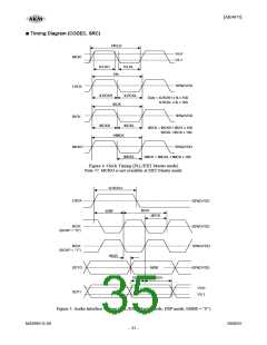
Note 69. I2C is a registered trademark of Philips Semiconductors.
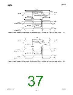
Note 70. In case that SAR ADC data is read out via I2C bus, SCL should be input corresponding 2 byte data including
ACK (Figure 110).
Note 71. Data must be held long enough to bridge the 300ns-transition time of SCL.
Note 72. CODEC & SRC blocks of the AK4675 can be reset by bringing PDN pin = “L” to “H” only upon power up
Note 73. This is the count of LRCK “↑” from the PMADL or PMADR bit = “1” when PMSRB bit = “0”.
Note 74. The signal path is SDTI → SRC-A → SDTOA and PLLBT is locked.
Note 75. The signal path is SDTIA → SRC-B → SDTO.
MS0963-E-00
2008/05
- 33 -

 AKM [ ASAHI KASEI MICROSYSTEMS ]