ASAHI KASEI
[AK4140]
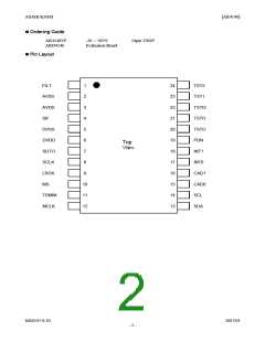
PIN/FUNCTION
No.
1
Pin Name
I/O Function
Filter Pin
FILT
-
2.2nF should be connected between FILT pin and VSS pin.
Analog Ground Pin
2
3
AVSS
-
-
AVDD
Analog Power Supply Pin, 2.7 ∼ 3.3V
4.5MHz SIF Input Pin.
4
SIF
I
Should be AC-coupled with 68nF.
Digital Ground Pin
5
6
DVSS
-
-
DVDD
Digital Power Supply Pin, 2.7 ∼ 3.3V
Audio Serial Data Output Pin
7
8
SDTO
SCLK
LRCK
MS
O
“L” Output at Power-down mode.
Audio Serial Data Clock Pin
I/O
I/O
I
“L” Output in Master Mode at Power-down mode.
Output Channel Clock Pin
9
“L” Output in Master Mode at Power-down mode.
Master/Slave Control Pin
10
11
“H”: Master Mode, “L”: Slave Mode
TDM Serial Data Input Pin
TDMIN
I
I
Should be connected to “L” in normal mode.
Master Clock Input Pin
12
13
14
15
MCLK
SDA
SCL
I/O Control Data Pin.
I
Control Data Clock Pin.
CAD0
CAD1
INT0
I
Chip Address Pin 0
Chip Address Pin 1
Interrupt Pin 0
16
17
18
I
O
O
INT1
Interrupt Pin 1
Power Down Mode Pin
19
PDN
I
“H”: Power up, “L”: Power down and reset. The AK4140 must be reset once upon
power-up.
Test Output Pin
20
21
22
23
24
TSTO
TSTI1
TSTI2
TST1
TST2
O
I
Should be open.
Test Input Pin 1 (pull-down pin. typ: 150k ohm.)
Should be connected to DVSS.
Test Input Pin 2
I
Should be connected to DVSS.
Test Mode Pin 1 (pull-down pin. typ: 150k ohm.)
Should be connected to DVSS.
I
Test Mode Pin 2 (pull-down pin. typ: 150k ohm.)
Should be connected to DVSS.
I
MS0547-E-01
2007/03
- 3 -

 AKM [ ASAHI KASEI MICROSYSTEMS ]