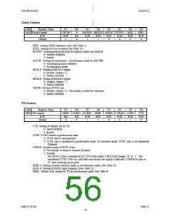
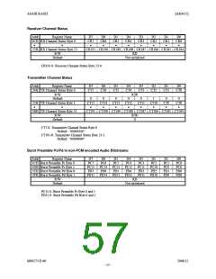
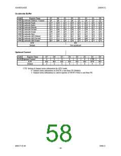
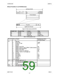
ASAHI KASEI
[AK4115]
SYSTEM DESIGN
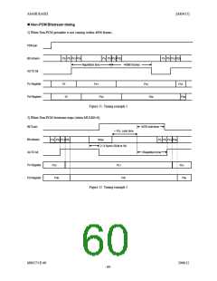
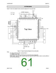
Figure 53 shows the example of system connection diagram for 4-wire serial mode.
3.3V
S/PDIF Sources
C1: 0.1µ
C2
+
C2: 10µ
C1
4.7µ
C1
C1
+
10kΩ
64
63
62
61
60
59
58
57
56
55
54
53
52
51
50
49
100p
10n
24kΩ
1
2
3
4
5
6
7
8
9
RX5
FILT 48
TEST(AVSS)
RX6
XTL1 47
XTL0 46
PSEL 45
IIC 44
PDN
RX7
C2 C1
+
DVDD
VIN
BVSS 43
DVSS 42
DVDD 41
CSN 40
3.3V
C1 + C2
DAUX
DVSS
3.3V
Top View
10 MCKO1
11 MCKO2
12 OVDD
13 OVSS
14 BICK
CCLK 39
CDTI 38
CDTO 37
INT1 36
INT0 35
ELRCK 34
EMCK 33
uP
DSP1
C1
15 SDTO
16 LRCK
DSP2
17
18
19
20
21
22
23
24
25
26
27
28
29
30
31
32
C1
C2
C1
+
+
C
C
C
C
uP
C2
S/PDIF out
5V
3.3V
Figure 53. Typical Connection Diagram (4-wire serial mode)
Notes:
- For setting of XTL0 and XTL1, refer the Table 13.
- “C” depends on the crystal.
- AVSS, BVSS, TVSS, OVSS and DVSS must be connected the same ground plane.
- Digital signals, especially clocks, should be kept away from the R and FILT pins in order to avoid an effect to
the clock jitter performance.
MS0573-E-00
2006/12
- 61 -

 AKM [ ASAHI KASEI MICROSYSTEMS ]