[AK1572]
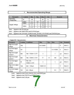
6. Absolute Maximum Rating
Parameter
Supply Voltage
Ground Level
Maximum RF Input Level RFPOW
Maximum Lo Input Level LOPOW
Analog Input Voltage
Digital Input Voltage1
Digital Input Voltage 2
Input Current
Symbol
Min.
Max.
Unit
Remarks
VDD1
VDD2
VDD3
VSS
-0.3
-0.3
-0.3
0
5.5
5.5
5.5
0
12
V
V
V
Note1, Note2
Note 3
Note4
Note5
Note6
Note7
V
dBm
dBm
V
V
V
mA
C
12
VAIN
VDIN1
VDIN2
IIN
VSS-0.3
VSS-0.3
VSS-0.3
-10
VDD3+0.3
VDD1+0.3
VDD3+0.3
10
Note1, Note8
Note1, Note9
Note1, Note10
Storage Temperature
Tstg
-55
125
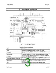
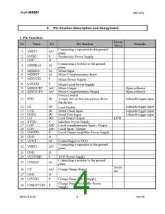
Note1 All voltage reference ground level: 0V
Note2 Applied to the [SVDD] pin
Note3 Applied to the [MIXVDD] and [LOVDD] pins
Note4 Applied to the [CPVDD], [CPBUFVDD], [PVDD], [VCOVDD] and [OAVDD] pins
Note5 Applied to the All [GND] pins
Note6 Applied to the [MIXINP] and [MIXINN] pins
Note7 Applied to the [LOP] and [LON] pins
Note8 Applied to the [VCNT] and [REFIN] pins
Note9 Applied to the [CLK], [DATA], [LE] and [PDN] pins
Note10 Applied to the [TEST1] and [TEST2] pins
Exceeding these maximum ratings may result in damage to the AK1572. Normal operation is not
guaranteed at these extremes.
MS1551-E-00
6
2013//8

 AKM [ ASAHI KASEI MICROSYSTEMS ]