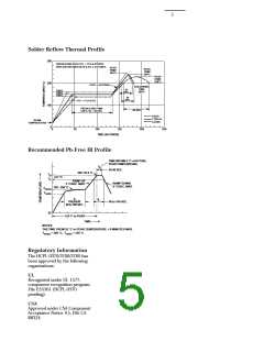
9
Notes:
1. Measured at a point 1.6 mm below seating plane.
2. Current into/out of any single lead.
3. Surge input current duration is 3 ms at 120 Hz pulse repetition rate. Transient input current duration is 10 µs at 120 Hz pulse
repetition rate. Note that maximum input power, PIN, must be observed.
4. Derate linearly above 70°C free-air temperature at a rate of 4.1 mW/°C (HCPL-3700/3760) and 3.1 mW/°C (HCPL-0370). Maximum
input power dissipation of 230 mW (HCPL-3700/3760) and 172 mW (HCPL-0370) allows an input IC junction temperature of 125°C
at an ambient temperature of TA = 70°C. Excessive PIN and TJ may result in IC chip degradation.
5. Derate linearly above 70°C free-air temperature at a rate of 5.4 mW/°C (HCPL-3700/3760) and 5 mW/°C (HCPL-0370).
6. Derate linearly above 70°C free-air temperature at a rate of 3.9 mW/°C (HCPL-3700/3760) and 1.9 mW/°C (HCPL-0370). Maximum
output power dissipation of 210 mW (HCPL-3700/3760) and 103 mW (HCPL-0370) allows an output IC junction temperature of
125°C at an ambient temperature of TA = 70°C.
7. Derate linearly above 70°C free-air temperature at a rate of 0.6 mA/°C.
8. Maximum operating frequency is defined when output waveform Pin 6 obtains only 90% of VCC with RL = 4.7 kΩ, CL = 30 pF using
a 5 V square wave input signal.
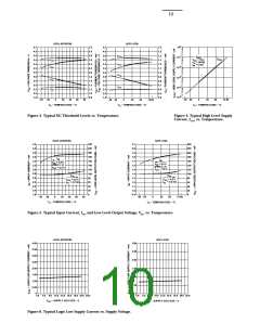
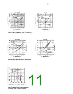
9. All typical values are at TA = 25°C, VCC = 5.0 V unless otherwise stated.
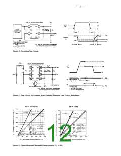
10. The tPHL propagation delay is measured from the 2.5 V level of the leading edge of a 5.0 V input pulse (1 µs rise time) to the 1.5 V
level on the leading edge of the output pulse (see Figure 10).
11. The tPLH propagation delay is measured from the 2.5 V level of the trailing edge of a 5.0 V input pulse (1 µs fall time) to the 1.5 V
level on the trailing edge of the output pulse (see Figure 10).
12. Common mode transient immunity in Logic High level is the maximum tolerable (positive) dVCM/dt on the leading edge of the
common mode pulse, VCM, to insure that the output will remain in a Logic High state (i.e., V > 2.0 V). Common mode transient
O
immunity in Logic Low level is the maximum tolerable (negative) dVCM/dt on the trailing edge of the common mode pulse signal,
V
CM, to insure that the output will remain in a Logic Low state (i.e., V < 0.8 V). See Figure 11.
O
13. In applications where dVCM/dt may exceed 50,000 V/µs (such as static discharge), a series resistor, RCC, should be included to
protect the detector IC from destructively high surge currents. The recommended value for RCC is 240 Ω per volt of allowable drop
in VCC (between Pin 8 and VCC) with a minimum value of 240 Ω.
14. Logic low output level at Pin 6 occurs under the conditions of VIN ≥ VTH+ as well as the range of VIN > VTH– once VIN has exceeded
VTH+ . Logic high output level at Pin 6 occurs under the conditions of VIN ≤ VTH- as well as the range of VIN < VTH+ once VIN has
decreased below VTH-
.
15. AC voltage is instantaneous voltage.
16. Device considered a two terminal device: Pins 1, 2, 3, 4 connected together, and Pins 5, 6, 7, 8 connected together.
17. In accordance with UL 1577, each optocoupler is proof tested by applying an insulation test voltage ≥ 4500 V rms for 1 second
(leakage detection current limit, Ii-o ≤ 5 µA).
18. In accordance with UL 1577, each optocoupler is proof tested by applying an insulation test voltage ≥ 6000 V rms for 1 second
(leakage detection current limit, Ii-o ≤ 5 µA). This test is performed before the 100% production test for partial discharge (Method b)
shown in the IEC/EN/DIN EN 60747-5-2 Insulation Characteristics Table.
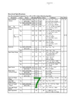
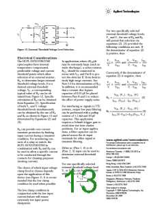
INPUT
DEVICE
TH+
TH–
CONNNECTION
ITH
HCPL-0370/3700 2.5 mA 1.3 mA
PINS 2, 3
OR 1, 4
HCPL-3760
ALL
1.2 mA 0.6 mA
VTH(dc)
VTH(ac)
3.7 V
4.9 V
2.6 V
3.7 V
PINS 2, 3
PINS 1, 4
ALL
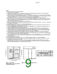
Figure 1. Typical Input
Figure 2. Typical Transfer Characteristics.
Characteristics, IIN vs. V (AC Voltage
is Instantaneous Value).IN

 AGILENT [ AGILENT TECHNOLOGIES, LTD. ]