6
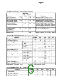
Insulation and Safety Related Specifications
8-Pin DIP
(300 mil)
Value
SO-8
Value Units
Parameter
Symbol
Conditions
Min.. External Air Gap
(External Clearance)
L(IO1)
7.1
4.9
4.8
mm Measured from input terminals to output
sterminals, hortest distance through air
Min.. External Tracking
Path (External Creepage)
L(IO2)
7.4
mm Measured from input terminals to output
terminals, shortest distance path along body
Min.. Internal Plastic
Gap (Internal Clearance)
0.08
0.08
mm Through insulation distance, conductor to
conductor, usually the direct distance between
the photoemitter and photodetector inside the
optocoupler cavity
Tracking Resistance
(Comparative
Tracking Index)
CTI
200
200
IIIa
V
DIN IEC 112/VDE 0303 PART 1
Isolation Group
Material Group (DIN VDE 0110, 1/89, Table 1)
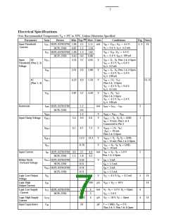
Absolute Maximum Ratings (No derating required up to 70°C)
Parameter
Storage Temperature
Symbol
TS
Min.
-55
Max.
125
85
Units
°C
Note
Operating Temperature
Lead Soldering Cycle
TA
-40
°C
Temperature
Time
260
10
°C
1
s
Input Current
Average
Surge
50
2
IIN
140
500
mA
2, 3
Transient
Input Voltage (Pins 2-3)
Input Power Dissipation
V
-0.5
V
IN
HCPL-3700/3760
HCPL-0370
PIN
PT
PO
IO
230
172
305
275
210
103
30
mW
4
5
6
7
Total Package Power Dissipation
Output Power Dissipation
HCPL-3700/3760
HCPL-0370
mW
mW
HCPL-3700/3760
HCPL-0370
Output Current
Average
mA
V
Supply Voltage (Pins 8-5)
Output Voltage (Pins 6-5)
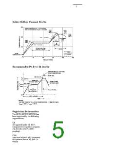
Solder Reflow Temperature Profile
V
CC
-0.5
-0.5
20
V
O
20
V
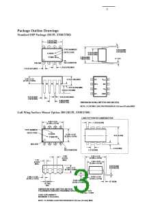
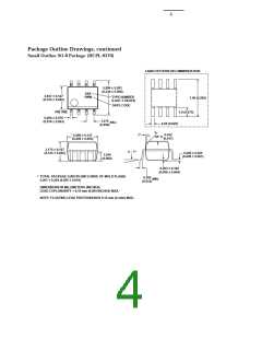
See Package Outline Drawings section
Recommended Operating Conditions
Parameter
Symbol
Min.
Max.
18
Units
Note
Supply Voltage
V
CC
2
0
0
V
°C
Operating Temperature
Operating Frequency
TA
f
70
4
kHz
8

 AGILENT [ AGILENT TECHNOLOGIES, LTD. ]