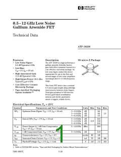
ATF-10236 Absolute Maximum Ratings
Notes:
Absolute
Maximum[1]
+5
1. Permanent damage may occur if
any of these limits are exceeded.
2. TCASE TEMPERATURE = 25°C.
3. Derate at 2.9 mW/°C for
TCASE >25°C.
4. Storage above +150°C may tarnish
the leads of this package making it
difficult to solder into a circuit.
After a device has been soldered
into a circuit, it may be safely
stored up to 175°C.
Symbol
VDS
VGS
VGD
IDS
PT
TCH
TSTG
Parameter
Units
V
Drain-Source Voltage
Gate-Source Voltage
Gate-Drain Voltage
Drain Current
Power Dissipation[2,3]
Channel Temperature
StorageTemperature[4]
V
V
mA
mW
°C
-4
-7
IDSS
430
175
175
°C
Thermal Resistance:
Liquid Crystal Measurement:
θjc =350°C/W;TCH =150°C
1µm Spot Size[5]
5. The small spot size of this tech-
nique results in a higher, though
more accurate determination of θjc
than do alternate methods. See
MEASUREMENTS section for
more information.
Part Number Ordering Information
Part Number
ATF-10236-TR1
ATF-10236-STR
Devices Per Reel
Reel Size
7"
1000
10
STRIP
For more information, see “Tape and Reel Packaging for Semiconductor Devices.”
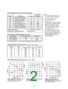
ATF-10236 Noise Parameters: VDS = 2 V, IDS = 25 mA
Γopt
Freq.
GHz
NFO
dB
RN/50
Mag
Ang
0.5
1.0
2.0
4.0
6.0
8.0
0.45
0.5
0.6
0.8
1.0
1.3
0.93
0.87
0.73
0.45
0.42
0.49
18
36
74
148
-137
-80
0.75
0.63
0.33
0.15
0.12
0.45
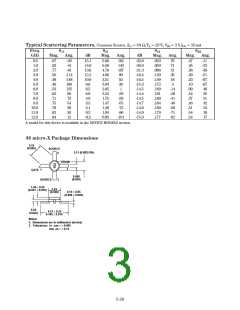
ATF-10236 Typical Performance, TA = 25°C
16
14
12
10
30
25
18
15
G
G
A
A
12
9
20
15
10
5
MSG
2
2.0
1.5
1.0
0.5
0
|S
|
1.5
1.0
0.5
0
21
6
MAG
NF
O
NF
O
0
0.5
2.0
4.0
6.0
8.0 10.0 12.0
0
10
20
30
40
50
60
1.0
2.0
4.0 6.0 8.0 12.0
FREQUENCY (GHz)
I
(mA)
FREQUENCY (GHz)
DS
Figure 2. Optimum Noise Figure and
Figure 3. Insertion Power Gain,
Maximum Available Gain and
Maximum Stable Gain vs. Frequency.
VDS = 2 V, IDS = 25 mA.
Figure 1. Optimum Noise Figure and
Associated Gain vs. Frequency.
VDS = 2V, IDS = 25 mA, TA = 25°C.
Associated Gain vs. IDS
.
VDS = 2V, f = 4.0 GHz.
5-27

 AGILENT [ AGILENT TECHNOLOGIES, LTD. ]