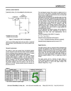
AMS1117
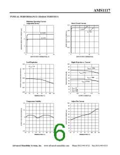
ELECTRICAL CHARACTERISTICS
Electrical Characteristics at IOUT = 0 mA, and TJ = +25°C unless otherwise specified.
Parameter
Device
Conditions
Min
Typ
Max
Units
Load Regulation
(Notes 2, 3)
AMS1117-2.85
3
6
12
20
mV
mV
VIN = 5V, 0 ≤ IOUT ≤ 1A
AMS1117-3.3
AMS1117-5.0
3
7
15
25
mV
mV
VIN = 5V, 0 ≤ IOUT ≤ 1A
VIN = 8V, 0 ≤ IOUT ≤ 1A
5
10
20
35
mV
mV
Dropout Voltage
AMS1117-1.5/-1.8/-2.5/-
2.85/-3.3/-5.0
V
1.1
1.3
∆VOUT , ∆VREF = 1%, IOUT = 1A (Note 4)
(VIN - V
)
OUT
Current Limit
AMS1117-1.5/-1.8/-2.5/-
2.85/-3.3/-5.0
(VIN - VOUT) = 5V
mA
900
1,100
1,500
Minimum Load
Current
AMS1117
(VIN - VOUT) = 12V (Note 5)
mA
mA
5
5
10
10
VIN ≤ 12V
Quiescent Current
AMS1117-1.5/-1.8/-2.5/-
2.85/-3.3/-5.0
Ripple Rejection
AMS1117
dB
dB
60
60
60
60
75
72
72
68
f =120Hz , COUT = 22µF Tantalum, IOUT = 1A,
(VIN-VOUT ) = 3V, CADJ =10µF
AMS1117-1.5/-1.8/-2.5/-
2.85
f =120Hz , COUT = 22µF Tantalum, IOUT = 1A,
VIN = 6V
AMS1117-3.3
dB
f =120Hz , COUT = 22µF Tantalum, IOUT = 1A
VIN = 6.3V
AMS1117-5.0
dB
f =120Hz , COUT = 22µF Tantalum, IOUT = 1A
VIN = 8V
Thermal Regulation
Adjust Pin Current
AMS1117
AMS1117
TA = 25°C, 30ms pulse
0.008
55
0.04
%W
10mA ≤ IOUT ≤ 1A , 1.5V≤ (VIN - VOUT) ≤ 12V
µA
µA
120
5
Adjust Pin Current
Change
AMS1117
0.2
10mA ≤ IOUT ≤ 1A , 1.5V≤ (VIN - VOUT) ≤ 12V
µA
Temperature Stability
Long Term Stability
RMS Output Noise
%
%
%
0.5
0.3
TA =125°C, 1000Hrs
1
0.003
TA = 25°C , 10Hz ≤ f ≤ 10kHz
(% of VOUT
)
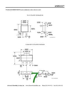
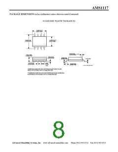
Thermal Resistance
Junction-to-Case
15
°C/W
Parameters identified with boldface type apply over the full operating temperature range.
Note 1: Absolute Maximum Ratings indicate limits beyond which damage to the device may occur. For guaranteed specifications and test conditions, see the
Electrical Characteristics. The guaranteed specifications apply only for the test conditions listed.
Note 2: Line and Load regulation are guaranteed up to the maximum power dissipation of 1.2 W. Power dissipation is determined by the input/output
differential and the output current. Guaranteed maximum power dissipation will not be available over the full input/output range.
Note 3: See thermal regulation specifications for changes in output voltage due to heating effects. Line and load regulation are measured at a constant junction
temperature by low duty cycle pulse testing. Load regulation is measured at the output lead ~1/8” from the package.
Note 4: Dropout voltage is specified over the full output current range of the device.
Note 5: Minimum load current is defined as the minimum output current required to maintain regulation. When 1.5V ≤ (VIN - VOUT) ≤ 12V the device is
guaranteed to regulate if the output current is greater than 10mA.
Advanced Monolithic Systems, Inc. www.advanced-monolithic.com Phone (925) 443-0722 Fax (925) 443-0723

 ADMOS [ ADVANCED MONOLITHIC SYSTEMS ]