ADV7180
of the ADC, 0 V to 1 V. This circuit should be placed before all
analog inputs to the ADV7180.
CSFM[2:0], C Shaping Filter Mode, Address 0x17 [7:5]
The C shaping filter mode bits allow the user to select from a
range of low-pass filters for the chrominance signal. When
switched in automatic mode, the widest filter is selected based
on the video standard/format and user choice (see Settings 000
and 001 in Table 33).
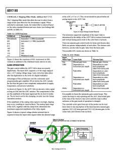
ANALOG VIDEO
INPUT
100nF
AIN_OF_ADV7180
36Ω
39Ω
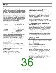
Figure 24. Input Voltage Divider Network
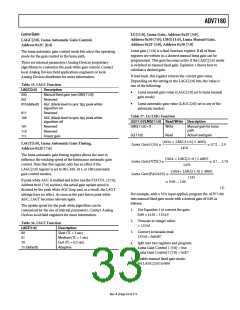
Table 33. CSFM Function
The minimum supported amplitude of the input video is
determined by the ability of the ADV7180 to retrieve horizontal
and vertical timing and to lock to the color burst, if present.
CSFM[2:0]
000 (default)
001
Description
Autoselect 1.5 MHz bandwidth
Autoselect 2.17 MHz bandwidth
There are separate gain control units for luma and chroma data.
Both can operate independently of each other. The chroma unit,
however, can also take its gain value from the luma path.
010
011
100
SH1
SH2
SH3
101
110
111
SH4
SH5
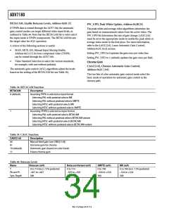
The possible AGC modes are shown in Table 34.
Table 34. AGC Modes
Input
Wideband mode
Figure 23 shows the responses of SH1 (narrowest) to SH5
(widest) in addition to the wideband mode (shown in red).
Video Type Luma Gain
Chroma Gain
Any
Manual gain luma
Manual gain chroma
CVBS
Dependent on
horizontal sync depth
Dependent on color-
burst amplitude
GAIN OPERATION
The gain control within the ADV7180 is done on a purely
digital basis. The input ADC supports a 10-bit range mapped
into a 1.0 V analog voltage range. Gain correction takes place
after the digitization in the form of a digital multiplier.
taken from luma path
Dependent on color-
burst amplitude
taken from luma path
Dependent on color-
burst amplitude
taken from luma path
Dependent on color-
burst amplitude
Peak white
Y/C
Dependent on
horizontal sync depth
Advantages of this architecture over the commonly used
programmable gain amplifier (PGA) before the ADC include
the fact that the gain is now completely independent of supply,
temperature, and process variations.
Peak white
YPrPb
Dependent on
horizontal sync depth
Taken from luma path
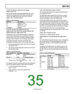
As shown in Figure 25, the ADV7180 can decode a video signal
as long as it fits into the ADC window. The components to this
are the amplitude of the input signal and the dc level it resides
on. The dc level is set by the clamping circuitry (see the Clamp
Operation section).
It is possible to freeze the automatic gain control loops. This
causes the loops to stop updating and the AGC determined gain
at the time of the freeze to stay active until the loop is either
unfrozen or the gain mode of operation is changed.
If the amplitude of the analog video signal is too high, clipping
may occur, resulting in visual artifacts. The analog input range
of the ADC, together with the clamp level, determines the
maximum supported amplitude of the video signal.
The currently active gain from any of the modes can be read
back. Refer to the description of the dual-function manual gain
registers, LG[11:0] luma gain and CG[11:0] chroma gain, in the
Luma Gain and Chroma Gain sections.
Figure 24 shows a typical voltage divider network that is
required to keep the input video signal within the allowed range
ANALOG VOLTAGE
RANGE SUPPORTED BY ADC (1V RANGE FOR ADV7180)
MAXIMUM
VOLTAGE
VIDEO PROCESSOR
(GAIN SELECTION ONLY)
DATA PRE-
PROCESSOR
(DPP)
ADC
GAIN
CONTROL
MINIMUM
VOLTAGE
CLAMP
LEVEL
Figure 25. Gain Control Overview
Rev. A | Page 32 of 112

 ADI [ ADI ]