ADV7180
TABLE OF CONTENTS
Features .............................................................................................. 1
SD Chroma Path......................................................................... 22
Sync Processing .......................................................................... 23
VBI Data Recovery..................................................................... 23
General Setup.............................................................................. 23
Color Controls............................................................................ 25
Clamp Operation........................................................................ 27
Luma Filter .................................................................................. 28
Chroma Filter.............................................................................. 31
Gain Operation........................................................................... 32
Chroma Transient Improvement (CTI) .................................. 36
Digital Noise Reduction (DNR) and Luma Peaking Filter... 37
Comb Filters................................................................................ 38
IF Filter Compensation ............................................................. 40
AV Code Insertion and Controls ............................................. 41
Synchronization Output Signals............................................... 43
Sync Processing .......................................................................... 50
VBI Data Decode ....................................................................... 50
I2C Readback Registers.............................................................. 59
Pixel Port Configuration ............................................................... 72
GPO Control................................................................................... 73
MPU Port Description................................................................... 74
Register Access............................................................................ 75
Register Programming............................................................... 75
I2C Sequencer.............................................................................. 75
I2C Register Maps ........................................................................... 76
I2C Programming Examples........................................................ 106
ADV7180 LQFP-64.................................................................. 106
ADV7180 LFCSP-40................................................................ 107
PCB Layout Recommendations.................................................. 108
Analog Interface Inputs........................................................... 108
Power Supply Decoupling ....................................................... 108
PLL ............................................................................................. 108
VREFN and VREFP................................................................. 108
Digital Outputs (Both Data and Clocks) .............................. 108
Digital Inputs ............................................................................ 108
Typical Circuit Connection......................................................... 109
Outline Dimensions..................................................................... 111
Ordering Guide ........................................................................ 111
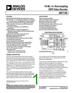
Applications....................................................................................... 1
Functional Block Diagram .............................................................. 1
General Description......................................................................... 1
Revision History ............................................................................... 3
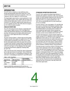
Introduction ...................................................................................... 4
Analog Front End......................................................................... 4
Standard Definition Processor ................................................... 4
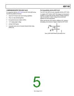
Comparison with the ADV7181B.............................................. 5
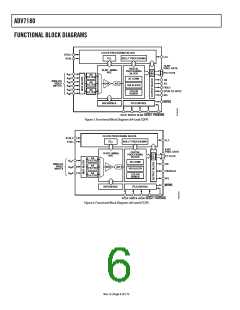
Functional Block Diagrams............................................................. 6
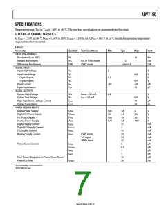
Specifications..................................................................................... 7
Electrical Characteristics............................................................. 7
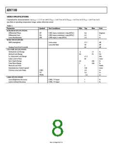
Video Specifications..................................................................... 8
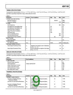
Timing Specifications .................................................................. 9
Analog Specifications................................................................... 9
Thermal Specifications ................................................................ 9
Timing Diagrams........................................................................ 10
Absolute Maximum Ratings.......................................................... 11
ESD Caution................................................................................ 11
Pin Configurations and Function Descriptions ......................... 12
40-Lead LFCSP ........................................................................... 12
64-Lead LQFP............................................................................. 13
Analog Front End ........................................................................... 15
Input Configuration................................................................... 16
INSEL[3:0], Input Selection, Address 0x00 [3:0] ................... 16
Analog Input Muxing ................................................................ 17
Antialiasing Filters ..................................................................... 18
Global Control Registers ............................................................... 19
Power-Saving Modes.................................................................. 19
Reset Control .............................................................................. 19
Global Pin Control ..................................................................... 19
Global Status Register .................................................................... 21
Identification............................................................................... 21
Status 1 ......................................................................................... 21
Autodetection Result.................................................................. 21
Status 2 ......................................................................................... 21
Status 3 ......................................................................................... 21
Video Processor .............................................................................. 22
SD Luma Path ............................................................................. 22
Rev. A | Page 2 of 112

 ADI [ ADI ]