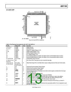
ADV7180
TIMING SPECIFICATIONS
Guaranteed by characterization. At AVDD = 1.71 V to 1.89 V, DVDD = 1.65 V to 2.0 V, DVDDIO = 3.0 V to 3.6 V, PVDD = 1.65 V to 2.0 V,
specified at operating temperature range, unless otherwise noted.
Table 4.
Parameter
Symbol Test Conditions
Min
Typ
Max
Unit
SYSTEM CLOCK AND CRYSTAL
Nominal Frequency
Frequency Stability
28.6363
MHz
ppm
50
I2C PORT
SCLK Frequency
400
kHz
μs
μs
μs
μs
ns
ns
ns
μs
SCLK Minimum Pulse Width High
SCLK Minimum Pulse Width Low
Hold Time (Start Condition)
Setup Time (Start Condition)
SDA Setup Time
SCLK and SDA Rise Times
SCLK and SDA Fall Times
Setup Time for Stop Condition
RESET FEATURE
t1
t2
t3
t4
t5
t6
t7
t8
0.6
1.3
0.6
0.6
100
300
300
0.6
Reset Pulse Width
5
ms
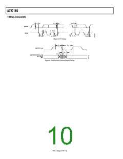
CLOCK OUTPUTS
LLC1 Mark Space Ratio
DATA AND CONTROL OUTPUTS
Data Output Transitional Time
t9:t10
45:55
55:45 % duty cycle
t11
t12
Negative clock edge to start of valid data
(tACCESS = t10 – t11)
End of valid data to negative clock edge
(tHOLD = t9 + t12)
3.6
2.4
ns
ns
Data Output Transitional Time
ANALOG SPECIFICATIONS
Guaranteed by characterization. At AVDD = 1.71 V to 1.89 V, DVDD = 1.65 V to 2.0 V, DVDDIO = 3.0 V to 3.6 V, PVDD = 1.65 V to 2.0 V,
specified at operating temperature range, unless otherwise noted.
Table 5.
Parameter
Test Conditions
Min
Typ
Max
Unit
CLAMP CIRCUITRY
External Clamp Capacitor
Input Impedance
Large-Clamp Source Current
Large-Clamp Sink Current
Fine Clamp Source Current
Fine Clamp Sink Current
0.1
10
0.4
0.4
10
μF
Clamps switched off
MΩ
mA
mA
μA
10
μA
THERMAL SPECIFICATIONS
Table 6.
Parameter
Symbol Test Conditions
Min
Typ
Max
Unit
THERMAL CHARACTERISTICS
Junction-to-Ambient Thermal
Resistance (Still Air)
Junction-to-Case Thermal Resistance
θJA
θJC
θJA
θJC
4-layer PCB with solid ground plane,
40-lead LFCSP
4-layer PCB with solid ground plane,
40-lead LFCSP
4-layer PCB with solid ground plane,
64-lead LQFP
30
3
°C/W
°C/W
°C/W
°C/W
Junction-to-Ambient Thermal
Resistance (Still Air)
Junction-to-Case Thermal Resistance
47
11.1
4-layer PCB with solid ground plane,
64-lead LQFP
Rev. A | Page 9 of 112

 ADI [ ADI ]