ADV7180
MAN_MUX_EN, Manual Input Muxing Enable,
ANALOG INPUT MUXING
Address 0xC4 [7]
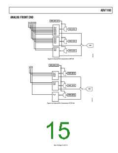
The ADV7180 has an integrated analog muxing section that
allows more than one source of video signal to be connected to
the decoder. Figure 9 and Figure 10 outline the overall structure
of the input muxing provided in the ADV7180.
To configure the ADV7180 analog muxing section, the user
must select the analog input AIN1 to AIN6 (ADV7180BSTZ) or
AIN1 to AIN3 (ADV7180BCPZ) that is to be processed by the
ADC. MAN_MUX_EN must be set to 1 to enable the following
muxing blocks:
A maximum of six CVBS inputs can be connected to and
decoded by the ADV7180BSTZ (64-lead LQFP) and a
maximum of three for ADV7180BCPZ (40-lead LFCSP). As
shown in the Pin Configurations and Function Description
section, these analog input pins lie in close proximity to one
another. This calls for a careful design of the PCB layout; for
example, ground shielding between all signals should be routed
through tracks that are physically close together. It is strongly
recommended to connect any unused analog input pins to
AGND to act as a shield.
•
•
•
MUX_0[3:0], ADC Mux Configuration, Address 0xC3 [3:0]
MUX_1[3:0], ADC Mux Configuration, Address 0xC3 [7:4]
MUX_2[3:0], ADC Mux Configuration, Address 0xC4 [3:0]
The three mux sections are controlled by the signal buses
SW_0/1/2[3:0]. Table 12 explains the control words used.
The input signal that contains the timing information (HS and
VS) must be processed by MUX_0. For example, in a Y/C input
configuration, MUX0 should be connected to the Y channel
and MUX1 to the C channel. When one or more muxes are not
used to process video, such as CVBS input, the idle mux and
associated channel clamps and buffers should be powered down
(see the description of Register 0x3A in Table 103).
Table 12. Manual Mux Settings for the ADC (MAN_MUX_EN Must be Set to 1)
ADC Connected to ADC Connected to
ADC Connected to
MUX_0[3:0]
000
001
010
011
LQFP-64
LFCSP-40
No connect
AIN1
No connect
No connect
AIN2
MUX_1[3:0]
000
001
010
011
LQFP-64
LFCSP-40
No connect
No connect
No connect
No connect
AIN2
MUX_2[3:0]
000
001
010
011
LQFP-64
LFCSP-40
No connect
No connect
No connect
No connect
No connect
AIN3
No connect
AIN1
AIN2
AIN3
AIN4
No connect
No connect
No connect
AIN3
AIN4
AIN5
No connect
No connect
AIN2
No connect
No connect
AIN5
100
101
100
101
100
101
AIN5
AIN3
AIN3
110
111
AIN6
No connect
No connect
No connect
110
111
AIN6
No connect
No connect
No connect
110
111
AIN6
No connect
No connect
No connect
Note the following:
•
•
•
CVBS can only be processed by MUX_0.
Y/C can only be processed by MUX_0 and MUX_1, respectively.
YPrPb can only be processed by MUX_0, MUX_1, and MUX_2, respectively.
Rev. A | Page 17 of 112

 ADI [ ADI ]