ADuC7019/20/21/22/24/25/26/27/28/29
Data Sheet
GENERAL DESCRIPTION
The devices operate from an on-chip oscillator and a PLL
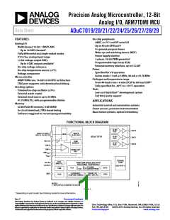
The ADuC7019/20/21/22/24/25/26/27/28/29 are fully integrated,
1 MSPS, 12-bit data acquisition systems incorporating high
performance multichannel ADCs, 16-bit/32-bit MCUs, and
Flash®/EE memory on a single chip.
generating an internal high frequency clock of 41.78 MHz
(UCLK). This clock is routed through a programmable clock
divider from which the MCU core clock operating frequency
is generated. The microcontroller core is an ARM7TDMI®,
16-bit/32-bit RISC machine, which offers up to 41 MIPS peak
performance. Eight kilobytes of SRAM and 62 kilobytes of
nonvolatile Flash/EE memory are provided on-chip. The
ARM7TDMI core views all memory and registers as a single
linear array.
The ADC consists of up to 12 single-ended inputs. An additional
four inputs are available but are multiplexed with the four DAC
output pins. The four DAC outputs are available only on certain
models (ADuC7020, ADuC7026, ADuC7028, and ADuC7029).
However, in many cases where the DAC outputs are not present,
these pins can still be used as additional ADC inputs, giving a
maximum of 16 ADC input channels. The ADC can operate in
single-ended or differential input mode. The ADC input voltage
is 0 V to VREF. A low drift band gap reference, temperature sensor,
and voltage comparator complete the ADC peripheral set.
On-chip factory firmware supports in-circuit serial download
via the UART or I2C serial interface port; nonintrusive emulation
is also supported via the JTAG interface. These features are
incorporated into a low cost QuickStart™ development system
supporting this MicroConverter® family.
Depending on the part model, up to four buffered voltage
output DACs are available on-chip. The DAC output range is
programmable to one of three voltage ranges.
The parts operate from 2.7 V to 3.6 V and are specified over an
industrial temperature range of −40°C to +125°C. When
operating at 41.78 MHz, the power dissipation is typically
120 mW. The ADuC7019/20/21/22/24/25/26/27/28/29 are
available in a variety of memory models and packages (see
Ordering Guide).
12-BIT
DAC0
DAC
ADC0 TO ADC4,
ADC12 TO ADC15
1MSPS
12-BIT ADC
MUX
12-BIT
ADuC7020
DAC1
DAC
TEMP
SENSOR
12-BIT
DAC2
DAC
CMP0
CMP1
BAND GAP
REF
12-BIT
DAC3
DAC
CMP
OUT
V
REF
3-PHASE
PWM
OSC
XCLKI
ARM7TDMI-BASED MCU WITH
AND PLL
ADDITIONAL PERIPHERALS
XCLKO
(SEE NOTE 1)
2k × 32 SRAM
31k × 16 FLASH/EEPROM
PLA
GPIO
JTAG
PSM
4 GENERAL-
PURPOSE TIMERS
SERIAL I/O
RST
POR
2
UART, SPI, I C
NOTES
1. SEE APPLICATION NOTE AN-798.
Figure 2.
Rev. F | Page 4 of 104

 ADI [ ADI ]