ADM3055E/ADM3057E
Data Sheet
APPLICATIONS INFORMATION
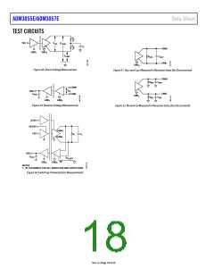
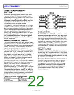
PCB LAYOUT
ADM3055E/
ADM3057E
Power supply bypassing is required at the logic input supply,
VIO, and at the shared CAN transceiver and digital isolator
input supply pin, VISOIN. Low equivalent series resistance (ESR)
bypass capacitors are required and must be placed as close to
the chip pads as possible. The ADM3055E and the ADM3057E
signal and power isolated CAN transceivers do not require
external interface circuitry for the logic interfaces.
1
2
20
19
18
17
16
15
14
13
12
11
10µF 0.1µF
0.1µF 0.01µF
GND
GND
GND
1
1
ISO
ISOOUT
0.22µF
10µF
V
3
V
V
GND
CC
IO
ISO
FERRITES
0.01µF 0.1µF
4
AUX
OUT
5
RXD
V
ISOIN
6
SILENT
TXD
GND
2
7
CANH
CANL
RS
8
STBY
The integrated dc-to-dc converter supply input pin, VCC, requires
parallel 10 µF and 0.1 µF bypass capacitors placed close to the
pin. Noise suppression requires a low inductance, high frequency
capacitor. Ripple suppression and proper regulation require a
large value capacitor. Effective bypass capacitance is also
required on the isolated output supply pin, VISOOUT, for proper
operation of the integrated dc-to-dc converter. Note that the
total trace length between the ends of the low ESR capacitors
9
AUX
IN
R
SLOPE
10
GND
GND
1
2
Figure 33. Recommended PCB Layout
THERMAL ANALYSIS
The ADM3055E and the ADM3057E consist of six internal die
attached to a split lead frame with four die attach pads. For the
purposes of thermal analysis, the die are treated as a thermal
unit, with the highest junction temperature reflected in the θJA
value in Table 10. The θJA value is based on measurements taken
with the devices mounted on a JEDEC standard, 4-layer board
with fine width traces and still air. Under normal operating
conditions, the ADM3055E and the ADM3057E can operate at
full load across the full temperature range without derating the
output current.
and the input power supply pins, VCC, VIO, VISOIN, and VISOOUT
must not exceed 2 mm.
,
RADIATED EMISSIONS AND PCB LAYOUT
The ADM3055E and the ADM3057E signal and power isolated
CAN FD transceivers pass EN 55022 Class B by 6 dB on a 2-layer
PCB design with ferrite beads. Neither PCB stitching capacitance
nor high voltage surface-mounted technology (SMT) safety
capacitors are required to meet this emissions level.
INSULATION LIFETIME
The ADM3055E and the ADM3057E have an internal split pad
lead frame on the bus side to isolate noise generated by the dc-
to-dc converter from the transceiver. For best noise suppression,
filter both the VISOOUT power supply pin and GNDISO power
supply return pin for high frequency currents before routing
power to the transceiver. Use surface-mount ferrite beads in
series with the signals, as shown in Figure 33.
All insulation structures eventually break down when subjected
to voltage stress over a sufficiently long period of time. The rate
of insulation degradation is dependent on the characteristics of
the voltage waveform applied across the insulation as well as on
the materials and material interfaces.
The two types of insulation degradation of primary interest are
breakdown along surfaces exposed to the air and insulation
wear out. Surface breakdown is the phenomenon of surface
tracking and is the primary determinant of surface creepage
requirements in system level standards. Insulation wear out
is the phenomenon where charge injection or displacement
currents inside the insulation material cause long-term
insulation degradation.
The isoPower integrated dc-to-dc converters of the ADM3055E
and the ADM3057E produce a 180 MHz carrier frequency to
transmit power through the chip scale transformer. The
impedance of the ferrite bead must be approximately 2 kΩ
between the 100 MHz and 1 GHz frequency range to reduce the
emissions of the 180 MHz primary switching frequency and
360 MHz secondary side rectifying frequency. See Table 14 for
examples of appropriate surface-mount ferrite beads. Although
the ferrite beads are beneficial for emissions performance, the
ferrite beads are not required for functionality.
Table 14. Surface-Mount Ferrite Beads Example
Manufacturer
Taiyo Yuden
Murata Electronics
Part No.
BKH1005LM182-T
BLM15HD182SN1
Rev. A | Page 22 of 24

 ADI [ ADI ]