ADM1026
PIN CONFIGURATION AND FUNCTION DESCRIPTIONS
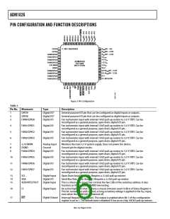
1
2
A
(0V – 3V)
PIN 1 IDENTIFIER
36
35
34
33
32
31
30
29
28
27
26
25
GPIO9
GPIO8
IN5
A
(0V – 2.5V)
(0V – 2.5V)
IN6
3
A
FAN0/GPIO0
FAN1/GPIO1
FAN2/GPIO2
FAN3/GPIO3
3.3V MAIN
DGND
IN7
+V
4
CCP
5
+12 V
–12 V
+5 V
IN
ADM1026
6
IN
TOP VIEW
7
(Not to Scale)
IN
VBAT
8
D2+/A (0V – 2.5V)
IN8
9
FAN4/GPIO4
FAN5/GPIO5
FAN6/GPIO6
FAN7/GPIO7
D2–/A (0V – 2.5V)
IN9
10
11
12
D1+
D1–/NTESTIN
Figure 3. Pin Configuration
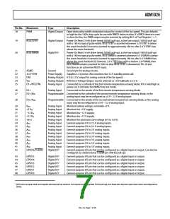
Table 3.
Pin No. Mnemonic
Type
Description
±
2
3
GPIO9
GPIO8
FAN0/GPIO0
Digital I/O±
Digital I/O±
Digital I/O
General-purpose I/O pin that can be configured as digital inputs or outputs.
General-purpose I/O pin that can be configured as digital inputs or outputs.
Fan tachometer input with internal ±0 kΩ pull-up resistor to 3.3 V STBY. Can be
reconfigured as a general-purpose, open drain, digital I/O pin.
4
5
6
FAN±/GPIO±
FAN2/GPIO2
FAN3/GPIO3
Digital I/O
Digital I/O
Digital I/O
Fan tachometer input with internal ±0 kΩ pull-up resistor to 3.3 V STBY. Can be
reconfigured as a general-purpose, open drain, digital I/O pin.
Fan tachometer input with internal ±0 kΩ pull-up resistor to 3.3 V STBY. Can be
reconfigured as a general-purpose, open drain, digital I/O pin.
Fan tachometer input with internal ±0 kΩ pull-up resistor to 3.3 V STBY. Can be
reconfigured as a general-purpose, open drain, digital I/O pin.
7
8
9
3.3 V MAIN
DGND
FAN4/GPIO4
Analog Input
Ground
Digital I/O
Monitors the main 3.3 V system supply. Does not power the device.
Ground pin for digital circuits.
Fan tachometer input with internal ±0 kΩ pull-up resistor to 3.3 V STBY. Can be
reconfigured as a general-purpose, open drain, digital I/O pin.
±0
±±
±2
FAN5/GPIO5
FAN6/GPIO6
FAN7/GPIO7
Digital I/O
Digital I/O
Digital I/O
Fan tachometer input with internal ±0 kΩ pull-up resistor to 3.3 V STBY. Can be
reconfigured as a general-purpose, open drain, digital I/O pin.
Fan tachometer input with internal ±0 kΩ pull-up resistor to 3.3 V STBY. Can be
reconfigured as a general-purpose, open drain, digital I/O pin.
Fan tachometer input with internal ±0 kΩ pull-up resistor to 3.3 V STBY. Can be
reconfigured as a general-purpose, open drain, digital I/O pin.
±3
±4
±5
SCL
SDA
ADD/NTESTOUT
Digital Input
Digital I/O
Digital Input
Open Drain Serial Bus Clock. Requires a 2.2 kΩ pull-up resistor.
Serial Bus Data. Open drain I/O. Requires a 2.2 kΩ pull-up resistor.
This is a three-state input that controls the two LSBs of the serial bus address. It also
functions as the output for NAND tree testing.
±6
±7
CI
Digital Input
An active high input that captures a chassis intrusion event in Bit 6 of Status Register 4.
This bit remains set until cleared, as long as battery voltage is applied to the VBAT input,
even when the ADM±026 is powered off.
INT
Digital Output Interrupt Request (Open Drain). The output is enabled when Bit ± of the configuration
register is set to ±. The default state is disabled. It has an on-chip ±00 kΩ pull-up resistor.
Rev. A | Page 6 of 56

 ADI [ ADI ]