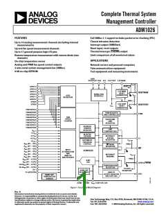
ADM1026
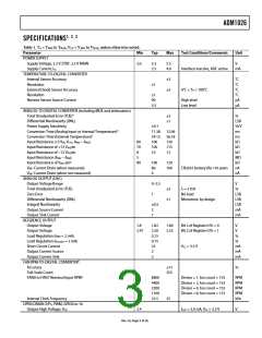
Parameter
Min
Typ
Max
±
0.4
Test Conditions/Comments
VOUT = VCC
IOUT = −3.0 mA, VCC = 3.3 V
Unit
µA
V
High Level Output Leakage Current, IOH
Output Low Voltage, VOL
PWM Output Frequency
0.±
75
Hz
DIGITAL OUTPUTS (INT, RESETMAIN, RESETBY)
Output Low Voltage, VOL
RESET Pulse Width
0.4
IOUT = −3.0 mA, VCC = 3.3 V
V
±40
2.2
±80
0.±
240
ms
OPEN DRAIN SERIAL DATABUS OUTPUT (SDA)
Output Low Voltage, VOL
High Level Output Leakage Current, IOH
SERIAL BUS DIGITAL INPUTS (SCL, SDA)
Input High Voltage, VIH
0.4
±
IOUT = –3.0 mA, VCC = 3.3 V
VOUT = VCC
V
µA
V
Input Low Voltage, VIL
0.8
V
Hysteresis
500
mV
DIGITAL INPUT LOGIC LEVELS (ADD, CI, FAN 0 to 7, GPIO 0 to ±6)7, 8
Input High Voltage, VIH
Input Low Voltage, VIL
Hysteresis (Fan 0 to 7)
2.4
0.8
VCC = 3.3 V
VCC = 3.3 V
VCC = 3.3 V
V
V
mV
250
RESETMAIN, RESETSTBY
RESETMAIN Threshold
2.89
3.0±
2.94
3.05
60
2.97
3.±0
Falling voltage
Falling voltage
V
RESETSBY Threshold
V
RESETMAIN Hysteresis
mV
mV
RESETSTBY Hysteresis
70
DIGITAL INPUT CURRENT
Input High Current, IIH
Input Low Current, IIL
Input Capacitance, CIN
EEPROM RELIABILITY
Endurance9
–±
VIN = VCC
VIN = 0
µA
µA
pF
±
20
±00
±0
700
kcycles
Years
Data Retention±0
SERIAL BUS TIMING
Clock Frequency, fSCLK
Glitch Immunity, tSW
Bus Free Time, tBUF
Start Setup Time, tSU; STA
Start Hold Time, tHD; STA
SCL Low Time, tLOW
SCL High Time, tHIGH
SCL, SDA Rise Time, tr
SCL, SDA Fall Time, tf
Data Setup Time, tSU; DAT
Data Hold Time, tHD; DAT
See Figure 2 for all parameters.
400
50
kHz
ns
µs
µs
µs
µs
µs
ns
ns
ns
ns
4.7
4.7
4
4.7
4
±000
300
250
300
± All voltages are measured with respect to GND, unless otherwise specified.
2 Typicals are at TA = 25°C and represent the most likely parametric norm. Shutdown current typ is measured with VCC = 3.3 V.
3 Timing specifications are tested at logic levels of VIL = 0.8 V for a falling edge and VIH = 2.± V for a rising edge.
4 Total unadjusted error (TUE) includes offset, gain, and linearity errors of the ADC, multiplexer, and on-chip input attenuators. VBAT is accurate only for VBAT voltages
greater than ±.5 V (see Figure ±5).
5 Total analog monitoring cycle time is nominally 273 ms, made up of ±8 ms × ±±.38 ms measurements on analog input and internal temperature channels, and
2 ms × 34.±3 ms measurements on external temperature channels.
6 The total fan count is based on two pulses per revolution of the fan tachometer output. The total fan monitoring time depends on the number of fans connected and
the fan speed. See the Fan Speed Measurement section for more details.
7 ADD is a three-state input that may be pulled high, low, or left open-circuit.
8 Logic inputs accept input high voltages up to 5 V even when device is operating at supply voltages below 5 V.
9 Endurance is qualified to ±00,000 cycles as per JEDEC Std. 22 method A±±7, and measured at −40°C, +25°C, and +85°C. Typical endurance at +25°C is 700,000 cycles.
±0 Retention lifetime equivalent at junction temperature (TJ ) = 55°C as per JEDEC Std. 22 method A±±7. Retention lifetime based on an activation energy of 0.6 V
derates with junction temperature as shown in Figure ±6.
Rev. A | Page 4 of 56

 ADI [ ADI ]