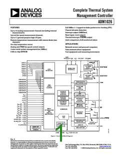
ADM1026
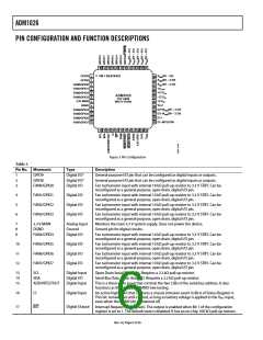
ABSOLUTE MAXIMUM RATINGS
Stresses above those listed under Absolute Maximum Ratings
may cause permanent damage to the device. This is a stress
rating only; functional operation of the device at these or any
other conditions above those indicated in the operational
section of this specification is not implied. Exposure to absolute
maximum rating conditions for extended periods may affect
device reliability.
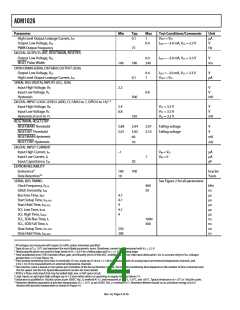
Table 2.
Parameter
Rating
Positive Supply Voltage (VCC
Voltage on +±2 V VIN Pin
Voltage on −±2 V VIN Pin
Voltage on Analog Pins
Voltage on Open Drain Digital Pins
Input Current at any Pin
Package Input Current
)
6.5 V
+20 V
−20 V
−0.3 V to (VCC + 0.3 V)
−0.3 V to +6.5 V
±5 mA
THERMAL CHARACTERISTICS
±20 mA
•
•
48-Lead LQFP package
Maximum Junction Temperature (TJ MAX
Storage Temperature Range
Lead Temperature, Soldering
Vapor Phase (60 sec)
Infrared (±5 sec)
ESD Rating, −±2 VIN Pin
)
±50°C
−65°C to +±50°C
θJA = 50°C/W, θJC = 10°C/W
2±5°C
200°C
±000 V
2000 V
ESD Rating, All Other Pins
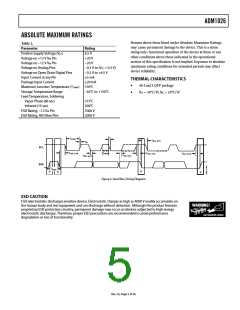
tF
tLOW
tHD; STA
tR
SCL
tHD; STA
tHIGH
tSU; STA
tSU; STO
tSU; DAT
tHD; DAT
SDA
tBUF
S
P
S
P
Figure 2. Serial Bus Timing Diagram
ESD CAUTION
ESD (electrostatic discharge) sensitive device. Electrostatic charges as high as 4000 V readily accumulate on
the human body and test equipment and can discharge without detection. Although this product features
proprietary ESD protection circuitry, permanent damage may occur on devices subjected to high energy
electrostatic discharges. Therefore, proper ESD precautions are recommended to avoid performance
degradation or loss of functionality.
Rev. A | Page 5 of 56

 ADI [ ADI ]