ADL5513
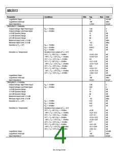
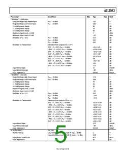
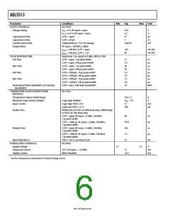
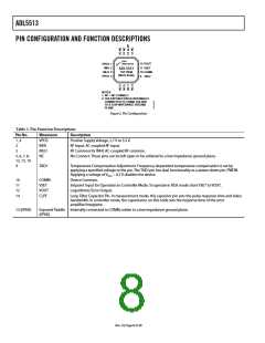
PIN CONFIGURATION AND FUNCTION DESCRIPTIONS
PIN 1
INDICATOR
12 VOUT
11 VSET
10 COMM
VPOS 1
INHI 2
ADL5513
TOP VIEW
(Not to Scale)
INLO 3
VPOS 4
9
TADJ
NOTES
1. NC = NO CONNECT.
2. THE EXPOSED PAD IS INTERNALLY
CONNECTED TO COMM; SOLDER
TO A LOW IMPEDANCE GROUND
PLANE.
Figure 2. Pin Configuration
Table 3. Pin Function Descriptions
Pin No.
Mnemonic
VPOS
INHI
Description
1, 4
2
Positive Supply Voltage, 2.7 V to 5.5 V.
RF Input. AC-coupled RF input.
3
INLO
RF Common for INHI. AC-coupled RF common.
5, 6, 7, 8,
NC
No Connect. These pins can be left open or be soldered to a low impedance ground plane.
13, 15, 16
9
TADJ
Temperature Compensation Adjustment. Frequency-dependent temperature compensation is set by
applying a specified voltage to the pin. The TADJ pin has dual functionality as a power-down pin, PWDN.
Applying a voltage of VPOS − 0.3 V disables the device.
10
11
12
14
COMM
VSET
VOUT
CLPF
Device Common.
Setpoint Input for Operation in Controller Mode. To operate in RSSI mode short VSET to VOUT.
Logarithmic/Error Output.
Loop Filter Capacitor Pin. In measurement mode, this capacitor pin sets the pulse response time and video
bandwidth. In controller mode, the capacitance on this node sets the response time of the error
amplifier/integrator.
15 (EPAD)
Exposed Paddle Internally connected to COMM; solder to a low impedance ground plane.
(EPAD)
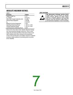
Rev. 0 | Page 8 of 28

 ADI [ ADI ]