ADL5513
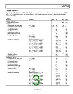
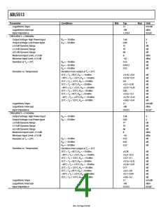
Parameter
Conditions
Min
Typ
Max
Unit
OUTPUT INTERFACE
Voltage Swing
Pin VOUT
VSET = 0 V, RF input = open
VSET = 0.47 V, RF input = open
CLPF = open
0.47
4.7
47
V
V
pF
nF
mA
Capacitance Drive
Capacitance Drive
Current Source/Sink
Output Noise
CLPF = 20 pF
1
Output held at 1 V to 1% change
RF input = 100 MHz, 0 dBm
fNOISE = 100 kHz, CLPF = open
0.64/55
145
82
nV/√Hz
nV/√Hz
f
NOISE = 100 kHz, CLPF = 1 nF
PULSE RESPONSE TIME
Fall Time
Input level = no signal to 0 dBm, 90% to 10%
CLPF = open, 1 µs pulse width
21
ns
CLPF = open, 500 µs pulse width
CLPF = open, 1 µs pulse width
5.5
20
20
4.2
5.5
3.2
4.3
10
µs
ns
ns
µs
µs
µs
µs
MHz
Rise Time
Fall Time
Rise Time
CLPF = open, 500 µs pulse width
CLPF = 1000 pF, 10 µs pulse width
CLPF = 1000 pF, 500 µs pulse width
CLPF = 1000 pF, 10 µs pulse width
CLPF = 1000 pF, 500 µs pulse width
CLPF = open, 3 dB video bandwidth
Small Signal Video Bandwidth (or Envelope
Bandwidth)
TEMPERATURE ADJUST/POWER-DOWN
INTERFACE
Pin TADJ
Temperature Adjust Useful Range
Minimum Logic Level to Disable
Input Current
0 to 1.3
VPOS − 0.3
31
V
V
mA
µA
Logic high disables
Logic high TADJ = 0 V
Logic low TADJ = 4.7 V
200
Enable Time
Disable Time
PWDN low to VOUT at 100% final value, PWDN high
to VOUT at 10% final value
CLPF = open, RF input = 0 dBm, 100 MHz,
1 µs pulse width
84
ns
µs
ns
µs
kΩ
10.8
165
1.2
13
CLPF = 1000 pF, RF input = 0 dBm, 100 MHz,
1 µs pulse width
CLPF = open, RF input = 0 dBm, 100 MHz,
1 µs pulse width
CLPF = 1000 pF, RF input = 0 dBm, 100 MHz,
1 µs pulse width
TADJ = 0.9 V, sourcing 70 µA
Pin VPOS
Input Impedance1
POWER SUPPLY INTERFACE
Supply Voltage
2.7
5.5
V
Quiescent Current
Supply Current
25°C, RF input = −55 dBm
When disabled
31
<0.2
mA
mA
1 See the Temperature Compensation of Output Voltage section.
Rev. 0 | Page 6 of 28

 ADI [ ADI ]