ADG406/ADG407/ADG426
ABSOLUTE MAXIMUM RATINGS
TA = 25°C unless otherwise noted.
Stresses above those listed under Absolute Maximum Ratings
may cause permanent damage to the device. This is a stress
rating only; functional operation of the device at these or any
other conditions above those indicated in the operational
section of this specification is not implied. Exposure to absolute
maximum rating conditions for extended periods may affect
device reliability.
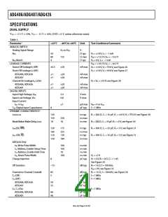
Table 3.
Parameter
Rating
VDD to VSS
44 V
VDD to GND
VSS to GND
Analog, Digital Inputs1
−0.3 V to +25 V
+0.3 V to −25 V
VSS − 2 V to VDD + 2 V or 20 mA,
whichever occurs first
ESD CAUTION
Continuous Current, S or D
Peak Current, S or D
20 mA
40 mA
(Pulsed at 1 ms, 10% duty
cycle max)
Operating Temperature Range
Industrial (B Version)
Storage Temperature Range
Junction Temperature
Plastic Package
−40°C to +85°C
−65°C to +150°C
150°C
θJA, Thermal Impedance
Lead Temperature, Soldering
(10 sec)
75°C/W
260°C
PLCC Package
θJA, Thermal Impedance
Lead Temperature, Soldering
Vapor Phase (60 sec)
Infrared (15 sec)
80°C/W
215°C
220°C
SSOP Package
θJA, Thermal Impedance
Lead Temperature, Soldering
Vapor Phase (60 sec)
Infrared (15 sec)
122°C/W
215°C
220°C
1
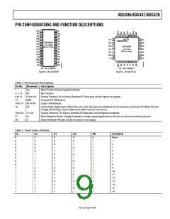
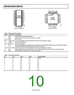
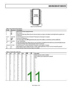
WR
RS
should be limited to the maximum ratings given.
Overvoltages at A, S, D,
, or will be clamped by internal diodes. Current
Rev. B | Page 8 of 20

 ADI [ ADI ]