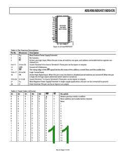
ADG406/ADG407/ADG426
V
1
2
3
4
5
6
7
8
9
28
27
D
DD
NC
RS
V
SS
26 S8
25 S7
24 S6
23 S5
22 S4
21 S3
20 S2
19 S1
18 EN
17 A0
16 A1
15 A2
S16
S15
S14
S13
S12
S11
ADG426
TOP VIEW
(Not to Scale)
S10 10
S9 11
GND 12
WR 13
A3 14
NC = NO CONNECT
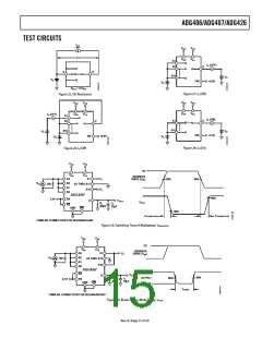
Figure 10. 28-Lead PDIP/SSOP
Table 8. Pin Function Descriptions
Pin No. Mnemonic Description
1
2
3
VDD
NC
RS
Most Positive Power Supply Potential.
No Connect.
Active Low Logic Input. When this pin is low, all switches are open, and address and enable latches registers are
cleared to 0.
4 to 11
12
S16 to S9
GND
Source Terminal 16 to Source Terminal 9. These pins can be inputs or outputs.
Ground (0 V) Reference.
13
WR
The rising edge of the WR signal latches the state of the address control lines and the enable line.
Logic Control Input.
Active High Digital Input. When this pin is low, the device is disabled and all switches are turned off. When this pin
is high, the Ax logic inputs determine which switch is turned on.
14 to 17 A3 to A0
18 EN
19 to 26 S1 to S8
Source Terminal 1 to Source Terminal 8. These pins can be inputs or outputs.
Most Negative Power Supply Potential. In single-supply applications, this pin can be connected to ground.
Drain Terminal. This pin can be an input or an output.
27
28
VSS
D
Table 9. Truth Table (ADG426)
WR
RS
A3
X
X
X
0
0
0
0
0
0
0
0
1
1
1
1
1
1
1
1
A2
X
X
X
0
0
0
0
1
1
1
1
0
0
0
0
1
1
1
1
A1
X
X
X
0
0
1
1
0
0
1
1
0
0
1
1
0
0
1
1
A0
X
X
X
0
1
0
1
0
1
0
1
0
1
0
1
0
1
0
1
EN
X
X
0
1
1
1
1
1
1
1
1
1
1
1
1
1
1
1
1
On switch
1
0
1
1
1
1
1
1
1
1
1
1
1
1
1
1
1
1
1
Retains previous switch condition
None (address and enable latches cleared)
None
1
2
3
4
5
6
7
8
9
10
11
12
13
14
15
16
X
0
0
0
0
0
0
0
0
0
0
0
0
0
0
0
0
0
Rev. B | Page 11 of 20

 ADI [ ADI ]