Data Sheet
ADA4627-1/ADA4637-1
C
F
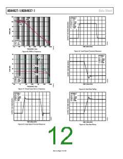
THD + N MEASUREMENTS
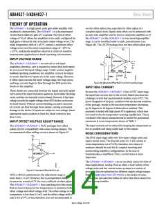
GUARD
Total harmonic distortion plus noise (THD + N) is usually
measured with an audio analyzer, such as those from Audio
Precision, Inc™. The analyzer consists of a low distortion
oscillator that is swept from the starting frequency to the
ending frequency. The oscillator is connected to the circuit
under test, and the output of the circuit goes back to the
analyzer.
R
F
2
3
6
+
OUT
–
ADA4627-1
V
I
8
N
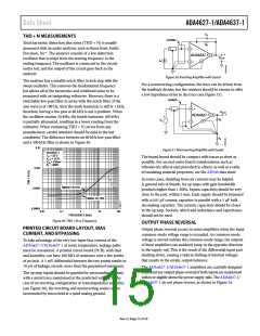
Figure 50. Inverting Amplifier with Guard
The analyzer has a tunable notch filter in lock step with the
swept oscillator. This removes the fundamental frequency
but allows all of the harmonics and wideband noise to be
measured with an integrating voltmeter. However, there is a
switchable low-pass filter in series with the notch filter. If the
sine wave is at 100 Hz, then the tenth harmonic is still at 1 kHz;
therefore, having a low pass at 80 kHz is not a problem. When
the oscillator reaches 20 kHz, the fourth harmonic (80 kHz)
is partially attenuated, resulting in a lower reading from the
voltmeter. When evaluating THD + N curves from any
manufacturer, careful attention should be paid to the test
conditions. The difference between an 80 kHz low-pass filter
and a 500 kHz filter is shown in Figure 49.
For a noninverting configuration, the trace can be driven from
the feedback divider, but the resistors should be chosen to offer
a low impedance drive to the trace (see Figure 51).
GUARD
3
V
OUT
6
+
ADA4627-1
+
–
R
F
V
8
S
2
R
I
–
0.01
Figure 51. Noninverting Amplifier with Guard
ADA4627-1
T
V
V
= 25°C
A
The board layout should be compact with traces as short as
possible. For second-order board considerations, such as
triboelectric effects and piezoelectric effects, as well as a table
of insulating material properties, see the AD549 data sheet.
= ±15V
= 810mV
= 600Ω
SY
IN
R
L
0.001
0.0001
In some cases, shielding from air currents may be helpful.
A general rule of thumb, for op amps with gain bandwidth
products higher than 1 MHz, bypass capacitors should be very
close to the part, within 3 mm. Each supply should be bypassed
with a 0.01 µF ceramic capacitor in parallel with a 1 µF bulk
decoupling capacitor. The ceramic capacitors should be closer
to the op amp. Sockets, which add inductance and capacitance,
should not be used.
500kHz FILTER
80kHz FILTER
0.00001
0.01
0.1
1
10
100
FREQUENCY (kHz)
Figure 49. THD + N vs. Frequency
OUTPUT PHASE REVERSAL
PRINTED CIRCUIT BOARD LAYOUT, BIAS
CURRENT, AND BYPASSING
Output phase reversal occurs in some amplifiers when the input
common-mode voltage range is exceeded. As common-mode
voltage is moved outside the common-mode range, the outputs
of these amplifiers can suddenly jump in the opposite direction
to the supply rail. This is the result of the differential input pair
shutting down, causing a radical shifting of internal voltages
that results in the erratic output behavior.
To take advantage of the very low input bias current of the
ADA4627-1/ADA4637-1 at room temperature, leakage paths
must be considered. A printed circuit board (PCB), with dust
and humidity, can have 100 MΩ of resistance over a few tenths
of an inch. A 1 mV differential between the two points results in
10 pA of leakage current, more than the guaranteed maximum.
The ADA4627-1/ADA4637-1 amplifiers are carefully designed
to prevent any output phase reversal if both inputs are maintained
within or slightly above the power supply rails. The ADA4627-1/
ADA4637-1 do not phase reverse, as shown in Figure 34.
The op amp inputs should be guarded by surrounding the nets
with a metal trace maintained at the predicted voltage. In the
case of an inverting configuration or transimpedance amplifier,
(see Figure 50), the inverting and noninverting nodes can be
surrounded by traces held at a quiet analog ground.
Rev. E | Page 15 of 20

 ADI [ ADI ]